To make atomically thin metals, just squeeze
DOI: 10.1063/pt.nthc.tuop

Since sticky tape was used just over two decades ago to isolate a single layer of graphene, an entire field of research has emerged to find more 2D materials, which have the thickness of just one or a few atoms. (See the article by Andrey Geim and Allan MacDonald, Physics Today, August 2007, page 35 .) Materials with atomic-scale dimensions exhibit distinct and exotic properties because of quantum confinement effects. Graphene, for example, has exceptionally high electrical conductivity because its structure hosts mobile electrons that behave like massless particles. (See Physics Today, December 2010, page 14 .)
Graphene provided a natural route into the realm of 2D materials because its one-atom-thick sheets have strong internal bonds but connect to other graphene sheets through weaker van der Waals forces. Those features make graphene relatively easy to peel off from its bulk form, graphite. Development of other 2D van der Waals materials, such as the insulating boron nitride and the semiconducting molybdenum disulfide (MoS2), has followed. (See the article by Pulickel Ajayan, Philip Kim, and Kaustav Banerjee, Physics Today, September 2016, page 38 .) Theory is used to predict some of the exotic properties of new 2D material phases. Under certain conditions, for example, 2D bismuth is expected to be a topological insulator—a material that conducts charge along its surfaces or edges while its interior acts as an insulator.
But bismuth, like other ordinary metals, is not thermodynamically stable as atomically thin sheets, so finding a way to make 2D materials out of it and other metals has not been straightforward. One approach to creating 2D metals has been to mix transition metals with carbon, nitrogen, or both—such mixtures make up a class of materials known as MXenes (pronounced Maxines, like the name; see Physics Today, June 2023, page 12 ). Very small pieces of pure metal films, ranging from nanometers up to about 10 μm across, have been synthesized using various other approaches, such as chemical vapor deposition, molecular-beam epitaxy, hot pressing, and growth confined between other 2D materials.
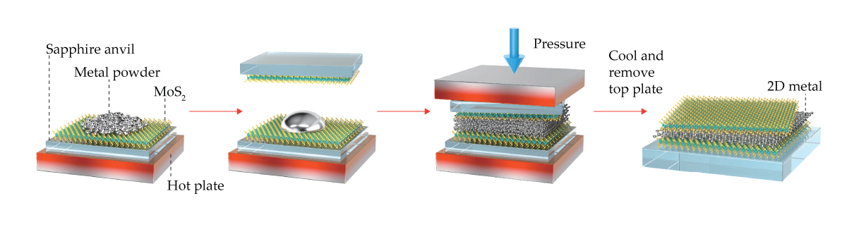
Figure 1.

Squeezing a molten metal between two sheets of molybdenum disulfide (MoS2) produces sheets of metal just two atoms thick. The MoS2, a van der Waals material that is stable as atomically thin sheets, provides a near-perfectly flat surface on which a 2D metal can be formed. Being encapsulated by MoS2 prevents the 2D metal from oxidizing but still allows access to the unique material properties that emerge because of quantum confinement effects that occur in atomic-scale materials. (Schematic adapted from ref.
Researchers have probed the material properties of those small pieces, but the samples are not large or uniform enough to be useful in engineered applications like microchips or qubits. Now, doctoral student Jiaojiao Zhao, his coadviser Luojun Du, lab director Guangyu Zhang, and their colleagues at the University of Chinese Academy of Sciences in Beijing and Songshan Lake Materials Laboratory in Dongguan, China, have created atomically thin metal sheets that are orders of magnitude larger by squeezing them with a hydraulic press. 1 “We have developed a very simple technique to prepare 2D metal, using an atomically flat surface to squeeze elements, and it works well,” says Zhang, who led the research.
A form of flattery
The atomically flat surfaces used to squeeze the metals are sapphire anvils fully coated with single layers of MoS2 and trimmed into 1 cm2 squares (see figure
As shown in figure
In addition to providing a flat surface to guide the pressed metals into a 2D form, the sheets of MoS2 also protect the metal from air. If one sheet of MoS2 is removed via reactive-ion etching, the metal quickly oxidizes and balls up. With the protection of the van der Waals material, though, the metal sheets are stable for at least a year.
Because the metals are not chemically bonded to the MoS2, their intrinsic electronic, optical, and magnetic properties can be probed—similar to the way that you can read what is written on a laminated a piece of paper. But at room temperature, MoS2 is a semiconductor. So to isolate the electronic properties of the confined metal, the researchers took measurements at cryogenic temperatures. At those low temperatures, MoS2 acts as an insulator and doesn’t contribute to the system’s conductivity.
Figure 2.

An atomically thin sheet of bismuth is more than 100 μm across, an order of magnitude larger than 2D metals that have been created by other approaches. Imaging of the edge of one such sheet (bottom left inset) reveals a two-atom-thick monolayer of bismuth sandwiched between sheets of molybdenum disulfide (MoS2). (Images adapted from ref.
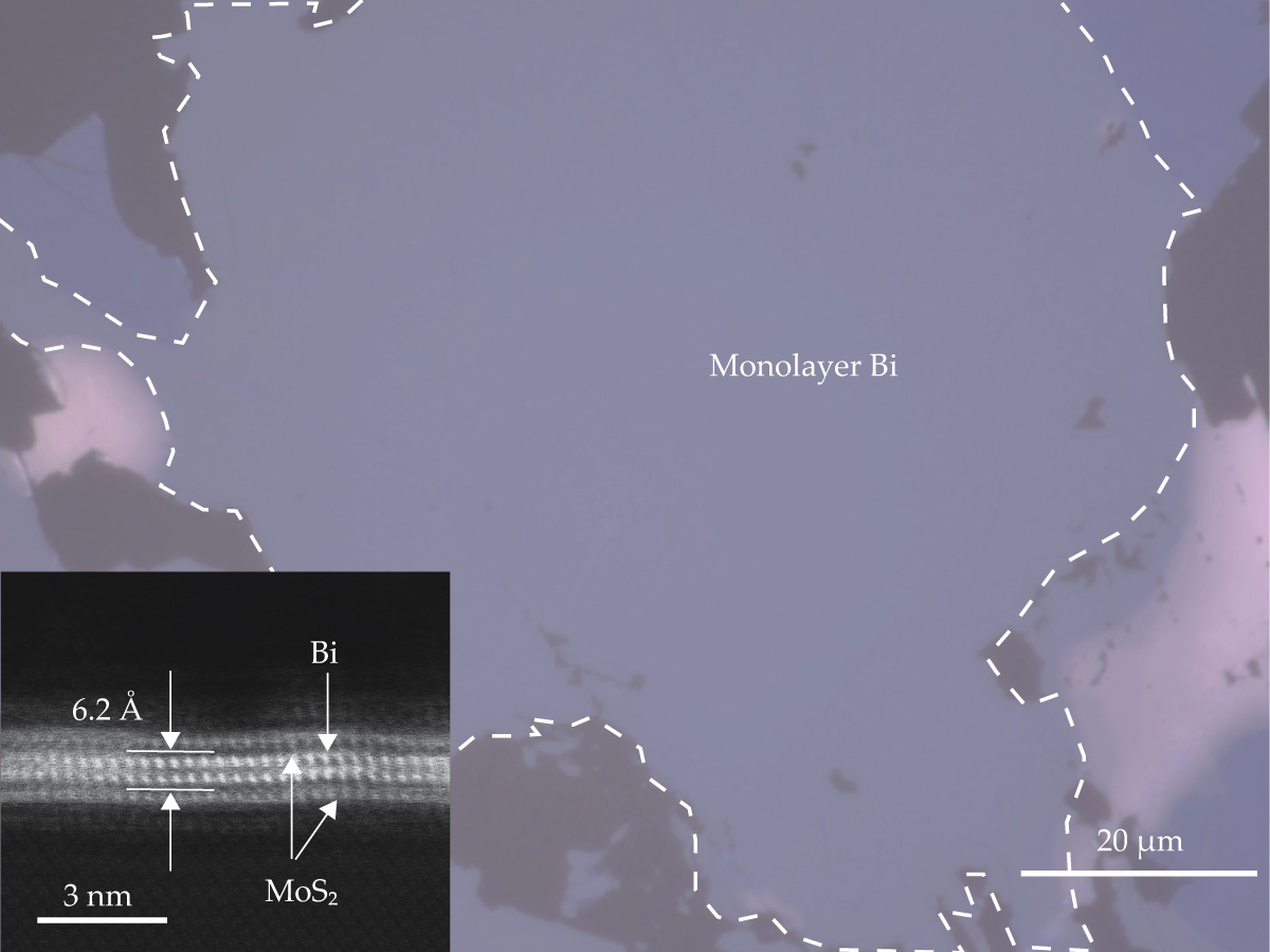
Zhao and colleagues used the squeezing technique to produce 2D sheets of bismuth, indium, tin, lead, and gallium. They focused their material characterization on 2D bismuth, which has been shown in previous studies (on smaller samples) to exhibit attractive properties, such as photoluminescence 2 and exceptional electronic transport. 3 By connecting the 2D bismuth to electrodes, the researchers observed electronic properties that aren’t seen in bulk metals. For example, the bismuth’s conductivity could be altered by an applied electric field in a phenomenon known as the field effect—a useful quality for building transistors.
Just a phase
The bismuth film produced in Zhao and colleagues’ study is, at its thinnest, two atoms thick. Those two atoms constitute a unit cell of the material’s rectangular crystal phase, the phase produced in the study. But many other phases can exist. A hexagonal phase of bismuth is predicted to have topological insulating properties at room temperature. Tweaking the fabrication technique’s conditions, such as the temperature or the angle between MoS2 sheets, could allow the creation of more material phases in the future.
Sheets of bismuth with four or six layers of atoms were produced when the researchers adjusted the pressure applied to the anvils. The researchers have had success with every single-element material they have tried the technique on, and their future work will investigate mixtures. “The first thing to do is study. We have almost no knowledge of these structures, 2D metals. We should first look at their fundamental properties,” says Zhang.
“It’s a great technological advance that can be applied to more materials,” says Princeton University’s Sanfeng Wu, who also works on the engineering of novel 2D metals. “I see a bright path forward for 2D metals and for techniques based on them to engineer quantum devices.”
By further refining the technique to produce extremely uniform surfaces to work with, the researchers may be able to create even larger metal sheets. The immense squeezing pressures inevitably scratch the steel plates used to compress the sapphire anvils, for example, so they must be polished back to a perfectly flat surface after each experiment. Any blemish in the surface can lead to the anvils fracturing at high pressures. But those are straightforward technological challenges Zhang is confident his lab can overcome.
“It’s not how people usually think about growing crystals—it’s a creative approach,” says Sanchez-Yamagishi. “It’s very cheap and simple compared to the million-dollar ultrahigh-vacuum systems which are typically used for growing thin crystals. Now that they’ve shown that it works, I expect other people to try.”
This article was originally published online on 11 April 2025.
References
1. J. Zhao et al., Nature 639, 354 (2025).https://doi.org/10.1038/s41586-025-08711-x
2. N. Hussain et al., Small 13, 1701349 (2017).https://doi.org/10.1002/smll.201701349
3. L. Chen et al., Nat. Mater. 23, 741 (2024).https://doi.org/10.1038/s41563-024-01894-0
More about the authors
Laura Fattaruso, lfattaruso@aip.org


