Electron microscopy for attosecond science
DOI: 10.1063/pt.owxp.nqan

The transmission electron microscope (TEM) is one of the most powerful imaging instruments. It works similarly to an optical microscope, but instead of using visible light, a TEM generates an accelerated electron beam that passes through a thin sample. The transmitted beam then interacts with a set of lenses that magnifies the sample image onto a camera detector. Because of diffraction limits, an optical microscope’s resolution can be no better than one-half the wavelength of light, or about 200 nm. But accelerated electrons in a TEM have much shorter wavelengths, making it possible to see 3D, atomic-scale features.

AMEÉ HENNIG
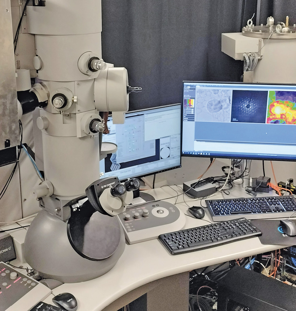
After the invention of the TEM in the early 1930s, for which some of its inventors were awarded the 1986 Nobel Prize in Physics, its imaging capabilities have been expanded significantly. In the TEM family of techniques, electron diffraction can be used to image crystallographic structure at subatomic resolution. Electron energy-loss spectroscopy (EELS) allows for imaging a sample’s core electronic structure and mapping its chemical elements. And cryoelectron microscopy—the development for which the 2017 Nobel Prize in Chemistry was awarded—enables researchers to determine the high-resolution structure of biomolecules in a cryogenic state (see Physics Today, December 2017, page 22 ).
On the temporal-resolution front, the TEM is limited by the video camera’s millisecond recording rate. The ultrafast electron microscope (UEM) overcomes that limit by using the TEM in a pump–probe approach. In that case, the camera’s recording rate becomes irrelevant to the temporal resolution, and the UEM is limited only by the duration of the ultrafast electron pulse.
The UEM is a tool that crosses disciplinary boundaries. It provides access to studying electronic, atomic, and molecular systems and their ultrafast dynamical processes, some of which range from picoseconds to a few hundred attoseconds.
Ultrafast electron microscopy
A typical ultrafast stroboscopic pump–probe measurement can capture processes that take place at the scale of hundreds of femtoseconds. The dynamics of a sample under study are triggered by the ultrafast pump pulse. Snapshots of the dynamics at different instants can then be recorded using ultrafast probe pulses that arrive at a sample at slightly different times after the triggering pump pulse. For the UEM, the pump and probe pulses are laser and electron pulses, respectively. To develop the UEM to image ultrafast processes, the design of the TEM needed modifications.
The continuous electron beam inside a TEM is usually generated from thermionic emission: Similar to how light is emitted from an incandescent bulb, electrons are generated by heating a filament. The UEM, to produce the ultrafast electron pulses it needs, replaces thermionic emission with photoemission. In the UEM, a photocathode of lanthanum hexaboride, when illuminated by UV laser pulses, will emit a beam of electron bursts, and the electron pulses have a duration comparable to that of the UV laser pulses.
The resulting temporal resolution of the UEM is a few hundred femtoseconds to a picosecond, defined mainly by the duration of the electron probe pulse, the duration of the pump pulse, and the timing jitter between the electron and laser pulses. To maintain the UEM’s temporal resolution, the jitter must be shorter in time than the duration of the electron pulse.
The duration of ultrafast electron pulses increases as the electrons travel farther from the photocathode to the sample. That’s because of the space-charge effect: As the electrons in the wavepacket move through the microscope, Coulomb repulsion among them causes some to travel faster than others and results in a longer pulse. In the UEM, the distance from the photocathode to the sample is fixed, which limits the temporal resolution to no better than a few hundred femtoseconds.
To overcome the space-charge effect, recent efforts have focused on implementing techniques that could compress the electron pulses and thus enhance the temporal resolution of the UEM. 1 One proposed approach is RF compression, which is based on slowing down the faster electrons and speeding up the slower ones. The output pulse, therefore, would have its electrons traveling closer to the same speed. The compressed electrons that exits the RF compressor would travel to the sample in a pulse that’s shorter than a few hundred femtoseconds. A proposed alternative to RF compression would use a deflection cavity inside the TEM. An electron beam passing through the cavity could be chopped into pulses of a few hundred femtoseconds for the UEM. 1
Figure
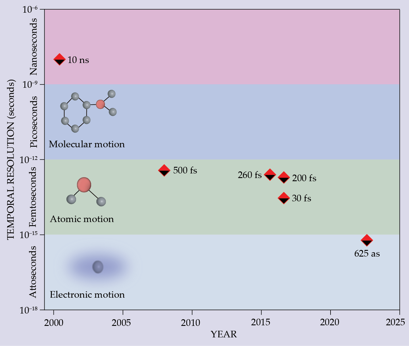
Figure 1.

Temporal resolution enhancements. Over the past several decades, the time scale at which the ultrafast electron microscope can operate has improved several orders of magnitude, from nanoseconds to hundreds of attoseconds. The developments open the door for imaging ultrafast molecular, atomic, and electron motions in action. (Sources, from longest: ref.
One of the most promising techniques uses a laser-driven emission gun: It produces a bright electron beam by illuminating with laser pulses a nanoscale tip. In another technique, adopted from conventional TEMs, cold field-emission guns that use the apex of a nanoemitter have been utilized in UEMs to generate bright electron pulses. 1 , 3 In both approaches, more-coherent electrons are generated by the photoemission process because it is localized at a nanotip emitter. In addition, researchers can control the photoemission process to be in the linear regime—in which each electron is emitted as a result of single-photon absorption from the UV pulse. That reduces the space-charge effect because all the electrons are emitted simultaneously and have the same energy distribution. The electron pulses that are generated using those techniques, therefore, have better spatiotemporal resolution than the typical UEM, which uses a lanthanum hexaboride source. 4 Because of the UEM’s advancement, many physical systems can be imaged at high temporal resolution.
Ultrafast imaging applications
UEM measurements connect ultrafast dynamics in a sample with the structural morphology of the sample.
5
The UEM, therefore, is a valuable tool in ultrafast science and has found different applications in chemistry, physics, materials science, and biology. In 2000, for example, a nanosecond electron microscope captured the laser-induced melting of a nickel–phosphorus metal thin film and the changing morphology of bulk cobalt in real space over time.
6
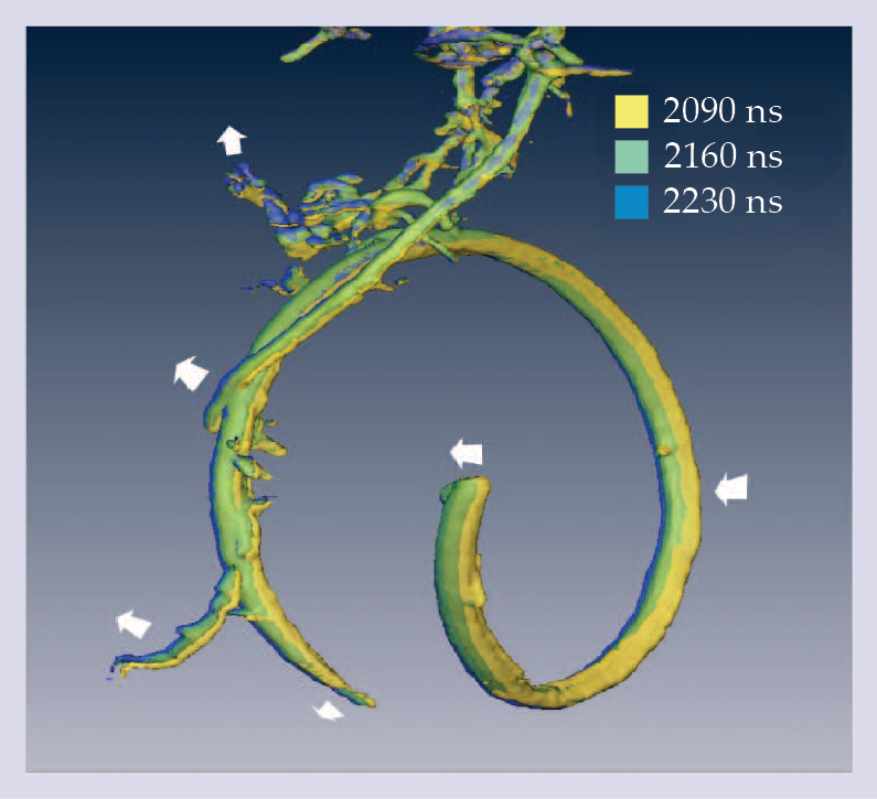
The images showed ultrafast behavior in the metals that wasn’t easily seen before with more typical optical pump–probe techniques. Moreover, the UEM has been used for imaging laser-triggered motion, such as the wiggling of ring structures of carbon nanotubes,
7
as shown in figure
Figure 2.

A carbon nanotube, roughly shaped like a ring, wiggles over a time scale of nanoseconds. Each color corresponds to a different snapshot in time, with white arrows indicating the local direction of motion. It’s one example of the imaging applications that have become possible because of advances in ultrafast electron microscopy. (Adapted from ref.
At the femtosecond time scale, the UEM has been used to look at ultrafast demagnetization. 8 In another study, the magnetic dynamics of bilayer films composed of iron and silicon nitride were probed, and the researchers demonstrated that stable magnetic nanoscale networks of vortices and antivortices could be produced. 9
Another imaging technique in the UEM family is EELS, which provides access to the electronic structure of matter at the valence and core levels with nanometer–femtosecond spatiotemporal resolution. The electronic-structure dynamics can be retrieved by tracing the EELS spectra as they change over time. One of the applications is the study of the photoinduced chemical-bonding dynamics in graphite. Researchers have found that even when the graphite’s crystal lattice contracts, some of the carbon–carbon bonds lengthen, which could explain various properties of the 2D system. 10
The applications of ultrafast electron microscopy extend to the study of dynamics in aqueous solution through the development of liquid-cell technology. Demonstrations include imaging the photoinduced rotational motion of gold nanoparticles in the liquid phase. With that development, the UEM could be helpful in studying ultrafast dynamics of biological systems in their native environments. In another example, cryoelectron microscopy was adopted into a UEM system to image picometer movements of photoresponsive biological structures embedded in ice. All the examples mentioned thus far have focused on processes that are no faster than hundreds of femtoseconds. To resolve still-faster processes, researchers had to exploit the subfemtosecond laser pulses of a recently developed microscopy imaging technique to generate equally short electron pulses.
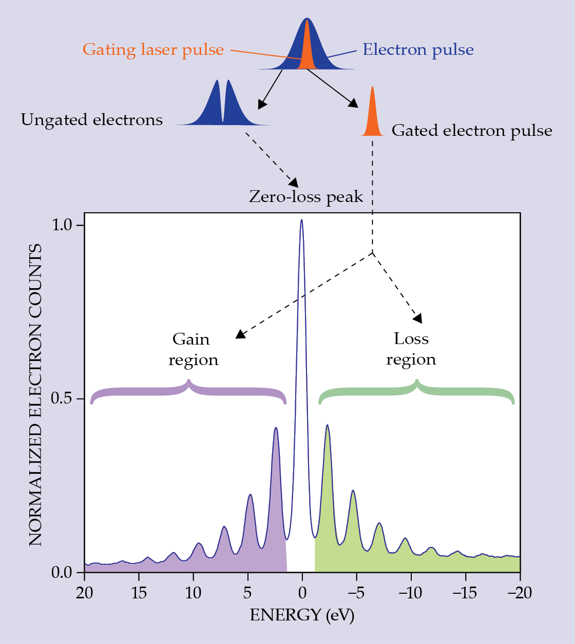
Photon–electron coupling
In a pioneering experiment published in 2009, the interaction between laser photons and free electrons was imaged by a UEM. 11 The photons that scatter off a nanostructure surface can exchange momentum with the microscope’s ultrafast pulse of free electrons, which lose and gain energy in integer multiples of photon quanta. The photon–electron coupling is resolved in the electron energy spectrum, which consists of discrete peaks that are spectrally separated by multiples of the photon energy. The approach, known as photon-induced near-field electron microscopy (PINEM), opens the door for various microscopy applications. 10
The PINEM technique, however, has another use. Recall that the temporal resolution of the UEM depends on the electron pulse duration inside the microscope, which has been limited to no better than a few hundred femtoseconds because of the space-charge effect. PINEM can break that limit and generate even-shorter electron pulses by what’s known as optical gating,
5
,
12
,
13
as shown in figure
Figure 3.

Making ultrafast electron pulses. In photon-induced near-field electron microscopy, an ultrafast laser pulse interacts with an electron pulse such that when the laser photons scatter off a nanostructure surface, they can exchange momentum with free electrons. The energy of electrons that interact elastically is at the zero-loss spectral peak. But the electrons coupled to photons have discrete electron energy peaks spectrally separated by multiples of the photon energy. Electrons that have gained and lost energy are correlated to the laser pulse and thus share its ultrafast temporal profile. That optical gating approach has been used to generate ultrashort electron pulses of a few hundred femtoseconds. (Adapted from ref.
The gated electron pulses can be used in a UEM to image dynamical processes that occur faster than hundreds of femtoseconds. The approach has been demonstrated, for example, to generate 30 fs electron pulses inside a microscope 12 and to image the phase transitions of vanadium oxide nanoparticles. 13
Attosecond electron microscopy
The optical-gating approach, in combination with laser pulses of a few hundred femtoseconds, has been exploited to generate a train of attosecond electron pulses inside a microscope. The laser pulses each consist of hundreds of half-cycle laser pulses, and each half-field cycle can optically gate electrons. That means that the gated electrons can form a train of electron pulses, and each pulse is confined to the subfemtosecond time scale for as long as the carrier frequency of the laser pulse is suitably high, in the visible or near-IR spectral region. In addition, a continuous-wave laser beam has been used to generate a train with an essentially infinite number of attosecond electron pulses. That approach has limited utility, though, and has been used for imaging only the periodic oscillations of scattered light. 14
As mentioned earlier, the temporal resolution of the UEM depends on the electron pulse’s duration, which defines the time window in which a dynamical process is probed. For a train of n electron pulses, the dynamical process will be probed n times during one pumping event. The recorded snapshots can be stacked to form a video of the average dynamics, as illustrated in figure
Figure 4.

Attosecond pulses. (a) A femtosecond electron pulse (yellow) is optically gated by a laser pulse to generate a train of attosecond pulses (blue), as described in figure
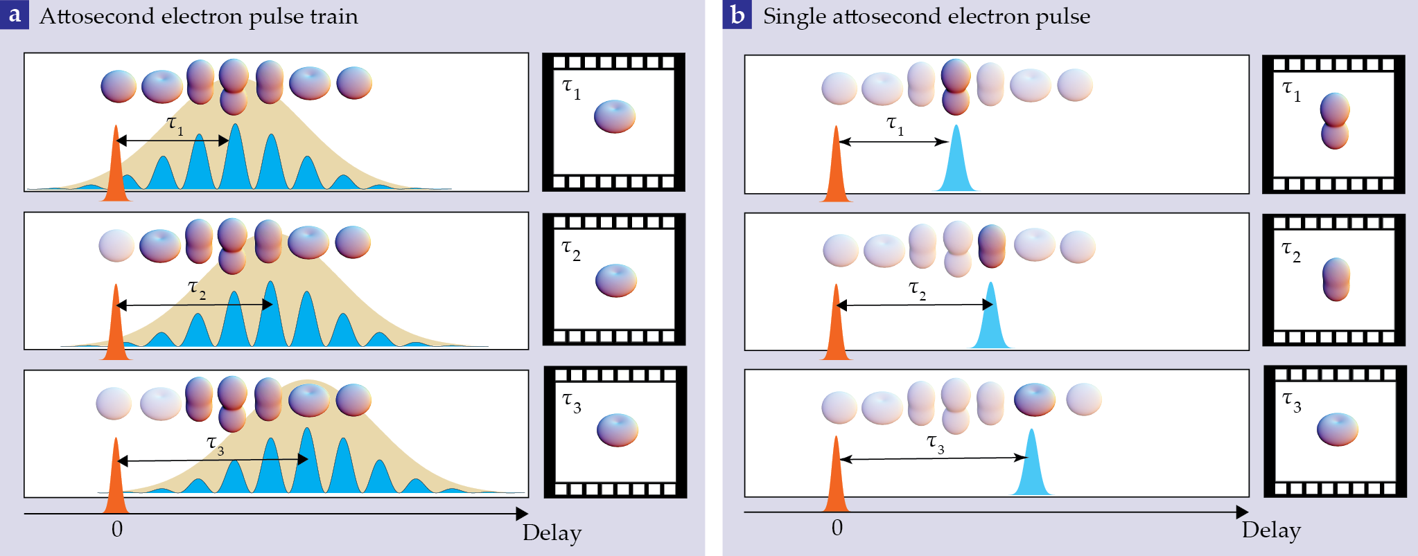
That sort of movie, however, won’t show the evolving motion produced by the pumping event in real time. Instead, the train of attosecond electron pulses is limited to imaging repeatable dynamics, such as the periodic oscillations of scattered light. The temporal resolution of the UEM remains the same as the temporal profile of the entire train of pulses. To resolve nonperiodic attosecond dynamics, such as electronic and atomic motions, a single attosecond electron pulse must be generated inside the microscope (see figure
In 2023 my research group generated a single attosecond electron pulse for imaging, which we call attomicroscopy by the polarization-gating approach. 5 , 15 We used it to probe the electron motion of carbon atoms in multilayer single-crystal graphene. 15 In polarization gating, a series of waveplates varies the laser’s polarization from linear to circular and then back to linear. At the instant of linear polarization, a strong, isolated attosecond pulse in the extreme UV can be generated via high-harmonic generation. 16 (For more on high-harmonic generation, see Physics Today, December 2023, page 13 . To learn about laser polarization and recollision theory, see the article by Paul Corkum, Physics Today, March 2011, page 36 .)
We used the polarization-gated laser pulse as an optical-gating pulse inside the microscope to generate the attosecond electron pulse. But polarization gating isn’t the only way to generate attosecond electron pulses. An optical attosecond pulse, which we demonstrated with a light-field synthesis method, 17 can also be used for attosecond gating of electrons inside the microscope. 5 , 17 , 18
Regardless of the method, the significance of generating attosecond temporal resolution in the electron microscope is the ability to image electron motion dynamics in real time. Although the spatial resolution of the UEM is still limited because of the space-charge effect, some indirect imaging approaches—such as attosecond time-resolved electron diffraction and EELS—can sidestep the space-charge effect and trace the electron motion in reciprocal space and the movement of valence electrons, respectively.
One of the most important advantages of attomicroscopy is the possibility of studying the electron dynamics of matter in neutral systems, which is difficult to do with other attosecond tools, such as extreme-UV laser pulses, because of the high photon energy and strong electric-field interaction that they require. Another advantage is that multiple measurements can be made on the same sample in one experiment: Attomicroscopy can observe ultrafast dynamics, and the normal TEM mode can directly image and characterize the sample’s morphology in real space. Thus I anticipate that attomicroscopy could be a powerful imaging tool for research in the development of nanoscale optoelectronics.
Viewing the microscopic world
Over the past two decades, the development of the UEM and the related technical advancements in spatiotemporal imaging resolution have led to many new findings in physics, chemistry, materials sciences, and biology. The full effect of the UEM on science and technology, however, remains unknown.
With the development of the optical-gating approach, I am optimistic that many groups will use the technology to study the ultrafast dynamics of a few tens to hundreds of femtoseconds. The new capability of attomicroscopy to probe field-induced electron motion dynamics would extend the capability of ultrafast electron microscopy to see the microscopic world of molecules, atoms, and electrons and their motion in real time and space.
Furthermore, attomicroscopy could be used in combination with cryoelectron microscopy to study electronic responses in biological systems, such as electron tunneling in DNA. Such imaging would help clarify the mechanism of electron tunneling between DNA strands and how it could change the structure of DNA. Attomicroscopy imaging, therefore, could be important to understanding carcinogenesis and mutagenesis mechanisms and the processes that repair damaged DNA.
Attosecond electron microscopy is already helping researchers investigate other biological phenomena, such as the electron movement that takes place between chains of cells through nanosized cable bacteria. Imaging the cables at attosecond temporal resolution could provide valuable insight for the design and construction of medical-compatible nanodevices. If implemented in the human body, the devices may be able to help detect, diagnose, and treat various diseases.
References
1. S. Borrelli et al., in Structural Dynamics with X-ray and Electron Scattering, K. Amini, A. Rouzée, M. J. J. Vrakking, eds., Royal Society of Chemistry (2024), p. 557.
2. P. E. Batson, N. Dellby, O. L. Krivanek, Nature 418, 617 (2002). https://doi.org/10.1038/nature00972
3. G. M. Caruso et al., Appl. Phys. Lett. 111, 023101 (2017). https://doi.org/10.1063/1.4991681
4. A. Feist et al., Ultramicroscopy 176, 63 (2017). https://doi.org/10.1016/j.ultramic.2016.12.005
5. M. T. Hassan, J. Phys. B 51, 032005 (2018). https://doi.org/10.1088/1361-6455/aaa183
6. O. Bostanjoglo et al., Ultramicroscopy 81, 141 (2000). https://doi.org/10.1016/S0304-3991(99)00180-1
7. O.-H. Kwon, A. H. Zewail, Science 328, 1668 (2010). https://doi.org/10.1126/science.1190470
8. K. B. Schliep et al., Appl. Phys. Lett. 110, 222404 (2017). https://doi.org/10.1063/1.4984586
9. T. Eggebrecht et al., Phys. Rev. Lett. 118, 097203 (2017). https://doi.org/10.1103/PhysRevLett.118.097203
10. E. Pomarico et al., MRS Bull. 43, 497 (2018). https://doi.org/10.1557/mrs.2018.148
11. B. Barwick, D. J. Flannigan, A. H. Zewail, Nature 462, 902 (2009). https://doi.org/10.1038/nature08662
12. M. T. Hassan et al., Nat. Photonics 11, 425 (2017). https://doi.org/10.1038/nphoton.2017.79
13. M. T. Hassan et al., Proc. Natl. Acad. Sci. USA 112, 12944 (2015). https://doi.org/10.1073/pnas.1517942112
14. D. Nabben et al., Nature 619, 63 (2023). https://doi.org/10.1038/s41586-023-06074-9
15. D. Hui et al., https://arxiv.org/abs/2305.03014 .
16. G. Sansone et al., Science 314, 443 (2006). https://doi.org/10.1126/science.1132838
17. M. T. Hassan et al., Nature 530, 66 (2016). https://doi.org/10.1038/nature16528
18. D. Hui et al., Nat. Photonics 16, 33 (2022); https://doi.org/10.1038/s41566-021-00918-4
H. Alqattan et al., APL Photonics 7, 041301 (2022). https://doi.org/10.1063/5.0082958
More about the authors
Mohammed Hassan is an associate professor of physics at the University of Arizona in Tucson. (Photo courtesy of Ameé Hennig.)


