US condensed-matter community grapples with availability of crystalline samples
DOI: 10.1063/1.2774089

The US “is a second-class, if not a third-class, citizen” in terms of investment in the synthesis of high-temperature superconductors, heavy-fermion materials, thin films, single crystals, ultra-pure semiconductors, and other specialized samples for condensed-matter experiments, says Cornell University’s Séamus Davis. US scientists “have to go cap in hand to the people who lead the development of new materials in these research fields.” Davis gets samples for his spectroscopic imaging scanning tunneling microscopy (STM) studies from colleagues in Japan, Canada, and the UK. “From the pure perspective of science,” he says, “things are great. It’s from the parochial perspective of how much belongs to the US that you may think there is a problem.”
With sample synthesis on the decline in the US over the past two decades or so, increasingly the US condensed-matter community does think there is a problem. Art Ramirez, director of device physics research at Bell Labs, notes that Bell, IBM, and a few other companies led the field after World War II. But around 1986, when the first observation of high-temperature superconductivity, by Georg Bednorz and Alex Möller in Switzerland, set off a rash of activity around the globe, “industrial investment in basic research began its rapid decline,” Ramirez says. “And no one has picked up the slack.”
The situation is reaching crisis proportions, says Jim Eisenstein of Caltech. The US, he adds, has been the leader in uncovering the physics of two-dimensional electron systems, and “the great majority of that success involved samples grown by one person at Bell Labs. It’s unstable to have only one individual at one institution making ultrahigh-purity semiconductor crystals—like everyone else, he will someday retire.” Worse, he says, what if Alcatel—which last year took over Bell’s parent company (see Physics Today, February 2007, page 26 )—pulls the plug?
A smattering of crystal growers work in national labs and universities across the US, but in recent years, concern in the condensed-matter community has been rising about the availability of samples, a future generation of sample growers, and competitiveness in the discovery and exploitation of new materials. A National Academy of Sciences report exploring these and related issues is due out next year.
The rub
At the University of British Columbia, Doug Bonn and colleagues have been tuning the high-temperature superconductor yttrium barium copper oxide for 18 years. Growing a sample can take a couple of months. “It’s never routine,” he says. “If a crystal is dirty, the subtle effects that test physicists’ theories are lost in the noise,” adds Loren Pfeiffer, the crystal grower at Bell Labs whom Eisenstein refers to. “The only difference between Klaus von Klitzing’s experiment and Horst Stormer and Dan Tsui’s experiment [which were awarded Nobel Prizes in 1985 and 1998 for the quantum Hall and fractional quantum Hall effects, respectively] was the crystal. Nothing else had changed.”
For the 21st century, adds Davis, “we need electronic materials that are patterned in different ways in real space. Many conventional materials—silicon, gold, aluminum—are translationally invariant. Their electronic structure in real space is completely boring.” What’s more, he says, to extend Moore’s law—the halving in size of electronic components every two years—“we need complex materials, for which the electronic structure is incredibly complicated, and you have to be able to see it in real space on the atomic scale before you can understand why it has the properties it does.” Making such materials, he adds, “is among the most challenging problems in physics, certainly in materials physics.”
Still, it’s the measurements, not the sample synthesis, that are generally recognized as “physics.” Says Pfeiffer, “To be considered a physicist, you have to do measurements. Some say that crystal growth is not physics, but you cannot conceive of the right crystal structure to grow without knowing the physics. Therein lies the rub.” Moreover, he adds, “very often, when I grow something for someone, it can take 20 iterations. The phase space is large: The density can be varied, the width of quantum wells, … there is literally an infinity of possibilities. The crystal grower is an intimate part of the collaboration.”
But getting tenure as a crystal grower is pretty much a nonstarter. “Crystal growers have hundreds of papers, but if you are talking about prizes, the notoriety goes to the people who make the measurements,” says Dale Van Harlingen of the University of Illinois at Urbana-Champaign. As a department chair, he adds, “If I can hire one person, I may not choose to hire a sample grower. He is going to grow samples and give them away. There is a reluctance to hire them. It’s a risk.”
“Growing crystals takes a lot of infrastructure. It’s difficult to support both a growing and measurement program,” says physicist Brian Maple of the University of California, San Diego. Maple, who is one of a handful of university-based crystal growers in the US, makes and characterizes single crystals and polycrystalline materials. In chemistry and materials science, he says, most crystal growers’ interests differ from physicists’.
Sample bottleneck
With samples hard to come by locally, US condensed-matter scientists often get them from abroad. “Many researchers become members in bigger collaborations that are often run from outside the US,” says Davis. This may work well for established scientists, says Robert Cava, a solid-state chemist who grows crystals at Princeton University, “but what about experimentalists who can’t get their hands on samples? Especially for young people, this is a problem. Getting good samples relies on nurturing contacts.”
“When you make a crystal, often the demand is exceedingly high,” says Pfeiffer. “Then you are in the tricky business of vetting colleagues.” Since growers of specialized samples tend to work in collaborations—rather than as supply houses—they generally don’t give the same type of sample to different researchers doing similar measurements. For example, Graeme Luke and his colleagues at McMaster University in Hamilton, Ontario, send crystalline samples for magnetic susceptibility, specific heat, thermal conductivity, optical conductivity, IR reflectance, and other measurements to a dozen groups around the world. “We don’t send many samples to neutron scattering or NMR [nuclear magnetic resonance] people in the US because we have good people here in our group, and we don’t send to their competitors,” says Luke. In STM, he adds, “Séamus [Davis] is the best in the world, and we give him samples. But if we hired an STM person, that person would get some priority.”
Demand for samples is only likely to increase as new facilities such as the Spallation Neutron Source at Oak Ridge National Laboratory ramp up. “Where are users of the SNS going to get samples?” asks Cava. “They are going to scrounge them.” Adds Luke, “You can have all the great advanced characterization facilities in the world. But it’s worthless if you don’t have high-quality samples to go in them.” And when top-flight facilities come on line in Japan, China, and elsewhere, US scientists will feel a squeeze.
Low cultural barrier, high payoff
In Japan, where the emphasis on materials took off at about the same time that synthesis in the US began to dwindle, many labs are equipped with several furnaces for growing samples. “Japan started a big investment in science during the bubble economy in the 1990s,” says Hidenori Takagi, a materials physicist at the University of Tokyo and the RIKEN research institute. “And even after the bubble went away, during the recession the government strengthened our science.” Takagi notes that in Japan, the “mental, or cultural, barrier between chemistry and physics is surprisingly low compared with the US, which is part of the reason why the bias against crystal growers [found in the US] is absent.” It also helps, he adds, that research groups in Japan tend to be bigger, “so you can work in both [sample growth and measurement].”
“You see lots of examples of people in physics departments [in Japan] who are involved in crystal growth—much more than in the US,” adds Harold Hwang, who in 2003 moved from Bell Labs to the University of Tokyo. Getting funding in Japan, he says, “is not a cakewalk, it’s competitive, but the distinction between synthesizing samples and making measurements is not there. Making samples is more highly valued here.”
One scientist in Japan who both grows crystals and measures their characteristics turns the prevailing logic in the US on its head: “Instead of saying crystal growers just make samples, and the hardcore physics lies in the measurements, you could say that any turkey can measure electrical properties, and the real insight is in knowing what sample to make.” The scientist, who requested anonymity, adds that either view is too extreme: “Advances in materials physics inherently involve the intimate coupling of both [crystal growth and measurements].”
“The key is that the Japanese recognize, intrinsically value, and therefore appropriately fund materials research in physics departments,” says Andy Mackenzie of Scotland’s University of St. Andrews. In Europe, attitudes about—and funding for—sample making are “intermediate between Japan and the USA, but closer to the USA,” he adds. Mackenzie launched his group’s materials growth activities with startup funds. “I doubt that any proposal could have succeeded unless I had made a promise to supply many people with many crystals,” he says. Likewise for Canada, adds Luke, “Temporarily the stars are aligned, but that could easily change.”
Japan’s high priority on materials has paid off, says Ramirez, ticking off a list of discoveries from Japan in the last 10 years of new materials with new physical properties: “Magnesium diboride, the 40-K superconductor; single-molecule organic metals; lithium vanadate, which was studied by folks in the US, but then the Japanese actually made crystals out of it, and it turns out to be the only 3d-orbital heavy-fermion system; water-doped superconductors; and on and on. It’s a whole slew of really exciting crystal growth successes.”
In being a leader in the field, Japan “gets first access to new materials, and they set the agenda,” says Ramirez. The cost of doing condensed-matter research is heavily weighted by big facilities, he adds. “The US put over a billion dollars into the SNS, and there is no commensurate increase in our ability to make materials. Which would you rather, set the agenda by spending a little bit of money, or spend a lot and not set the agenda?”
Seeking synthesis solutions
Joining the agenda setters in materials physics will take both money and structural changes. “I believe there is an evolving consensus that there’s a social aspect to the problem,” Pfeiffer says. Under discussion in the US condensed-matter community is whether to form national centers for crystal growth, perhaps collocated with the SNS and other facilities. Another approach would be to support crystal growing in physics departments. “It would be a nice way to nucleate new crystal growers. We should encourage people who have the talent. It would be part-time, but it would be motivated and focused on physics,” says Pfeiffer.
In 2003 the US Department of Energy sponsored a workshop called “Future Directions of Design, Discovery, and Growth of Single Crystals for Basic Research.” Following the workshop, says Harriet Kung, the director of materials sciences and engineering in DOE’s Office of Basic Energy Sciences, “we have made efforts to beef up single-crystal growth and augmented grants to increase capital equipment.” As a funding agency, she adds, DOE shares the responsibility for boosting the recognition of the need for materials discovery and synthesis, including in universities.
The current National Academy of Sciences study aims to assess the status of new materials synthesis and crystal growth in the US. Among the study’s charges are to identify areas of future research, consider the impact of such research on society, discuss the elements required for a nationally coordinated materials synthesis effort, and compare the levels of funding and effort in the field across several countries. “What we are looking for,” says Kung, “are concrete actionable recommendations, so I can use them as ammunition to argue for funding increases. If indeed there is a disparity in funding [between the US and other countries], that could help us make a case for increased investment.” Materials, she adds, “are the lynchpin for various energy technologies, so I can see design, discovery, and physics of new materials as a strong area for increasing investment.”

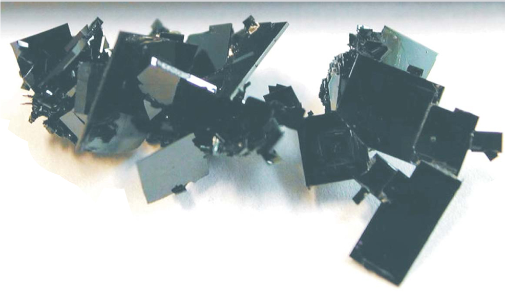
The high-temperature superconductor yttrium barium copper oxide is grown in crystal clusters; this one is about 2 cm from end to end. Typical experiments use single platelets from such clusters.
RUIXING LIANG

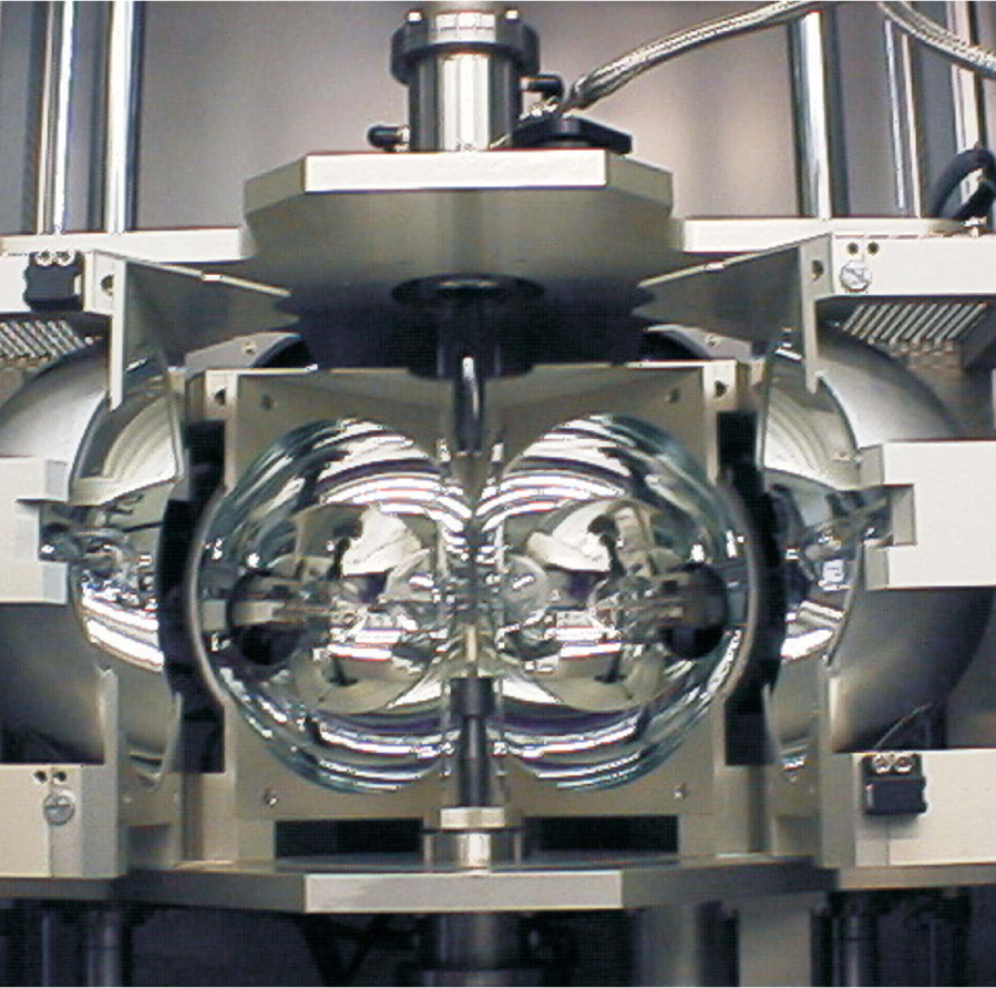
The floating zone crystal growth furnace is “arguably the best thing to happen to single-crystal growth in the past 25 years,” according to Princeton University’s Robert Cava. The US, he adds, doesn’t have enough of these machines by a factor of 10.
ROBERT CAVA

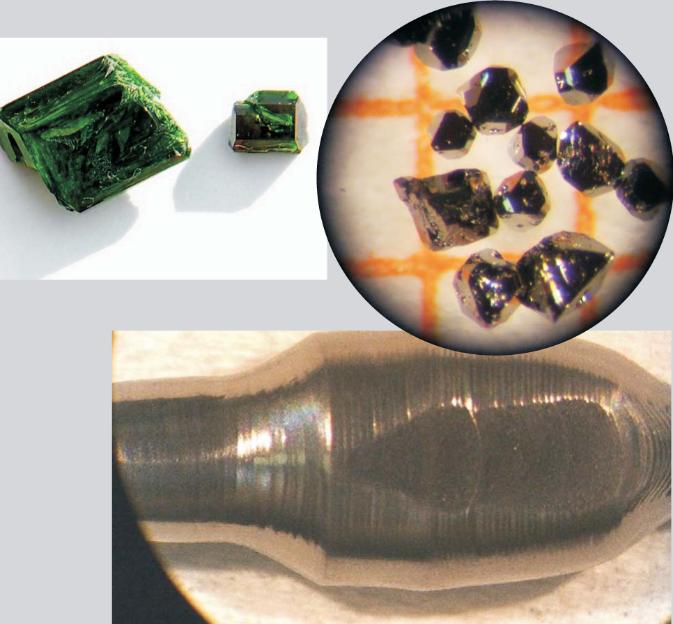
Crystals (clockwise from left): Nickel olivine (the larger crystal is roughly 1 cm long); single crystals of the filled-skutterudite praseodymium ruthenium arsenide (the orange square is 1 mm on a side); and a 4-cm-long specimen of the heavy-fermion superconductor uranium ruthenium silicide lightly doped with rhenium.
(Image at upper right courtesy of UCSD’s Brian Maple and Zygmunt Henkie, Institute of Low Temperature and Structure Research, Wroclaw, Poland.)

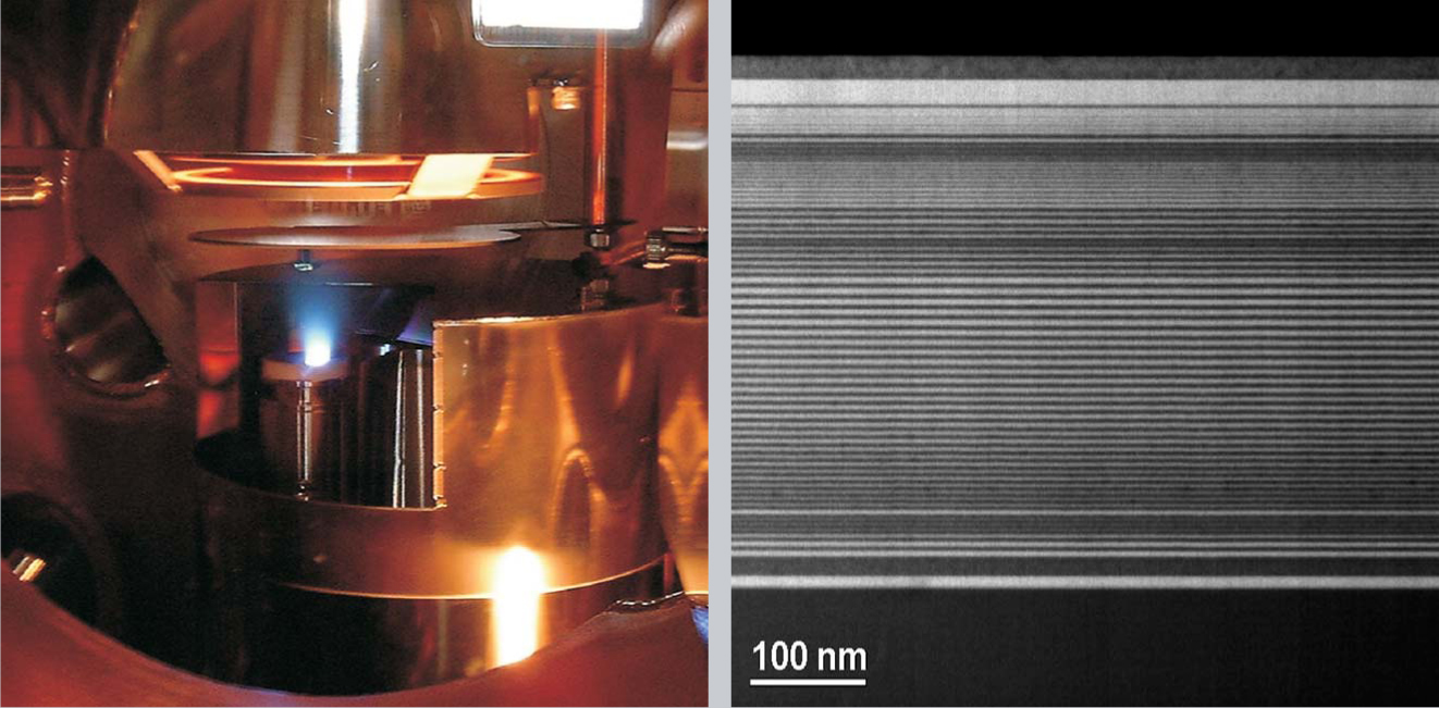
An ultrahigh vacuum pulsed laser deposition chamber (left) at the University of Tokyo was used to create a superlattice, whose thin layers of lanthanum vanadate and strontium titanate are bright and dark, respectively, in the scanning transmission electron microscopy image (right) made at Cornell University.
LENA FITTING KOURKOUTIS, YASUSHI HOTTA, DAVID A. MULLER, AND HAROLD Y. HWANG
More about the authors
Toni Feder, tfeder@aip.org


