Two Groups Observe the Spin Hall Effect in Semiconductors
DOI: 10.1063/1.1897513
In 1971, Mikhail Dyakonov and Vladimir Perel of the Ioffe Institute in Leningrad proposed a new transport phenomenon. 1 If one applies an electric field to the ends of a semiconducting strip, they reasoned, electrons would scatter off impurities in a spin-dependent way. As the electrons make their way along the strip, those with up spins would veer to one side, while those with down spins would veer to the other side.
The result is a transverse flow of spin, a “spin Hall effect.” Unlike the traditional Hall effect and its younger quantum cousins, the spin Hall effect doesn’t cause a transverse voltage. Nor does it need an external magnetic field. The polarization relies instead on the relativistic coupling of the electron’s spin and orbital angular momentum.
But the predicted polarization is modest. For two decades after its debut, Dyakonov and Perel’s proposal languished as a curiosity, all but ignored by theorists and experimenters alike.
Interest picked up when physicists began looking at ways to exploit electron spins to carry, store, and process information. Although magnetically controlled ferromagnets offer the easiest path to spin-based applications, electrically controlled semiconductors may have the greater potential. Electric fields can be produced and controlled on far shorter time scales and in far smaller volumes than magnetic fields can. And semiconductors, through gating, doping, and other techniques, are more adaptable materials than ferromagnets. In the envisioned world of semiconductor spintronics, the spin Hall effect looks like a useful tool to have.
In 1999, unaware of Dyakonov and Perel’s work, Jorge Hirsch of the University of California, Santa Cruz, came up with the same idea. 2 Then, in 2003, Shuichi Murakami and Naoto Nagaosa of the University of Tokyo and Shou-Cheng Zhang of Stanford University claimed that a potentially stronger and more useful spin Hall effect occurs even without impurities. 3 Independently and in parallel, Jairo Sinova of Texas A&M University, Allan MacDonald of the University of Texas at Austin, and their collaborators made a similar claim. 4 MacDonald coined the terms “intrinsic spin Hall effect” for the impurity-free version and “extrinsic spin Hall effect” for the impurity-dependent version.
The intrinsic effect proved controversial. More than 50 papers appeared arguing for or against its existence. But now at last, the spin Hall effect has been observed. Two independent groups—one based at the University of California, Santa Barbara; the other based at the Hitachi Laboratory in Cambridge, England—have reported convincing evidence that an electric field can indeed cause spins of opposite sign to accumulate on opposite sides of a semiconductor. 5,6 Intriguingly, the effect seen in Santa Barbara seems extrinsic, whereas the effect seen in Cambridge seems intrinsic.
Kerr probes and LEDs
The Santa Barbara team consists of David Awschalom, his graduate students Yuichiro Kato and Roberto Myers, and Art Gossard. To observe the spin Hall effect, they opted to use a Kerr probe. When linearly polarized light reflects off a magnetized surface, the light’s polarization axis rotates by an amount proportional to the magnetization: the Kerr effect. Mapping the polarization of light bouncing back from a strip of semiconductor would, in principle, reveal the telltale accumulation of up and down spins near the edges.
The team fashioned a strip of n-doped gallium arsenide 300 μm long, 77 μm wide, and 2.3 μm thick. To map the strip’s polarization, they imaged each 1 μm × 1 μm patch of the strip. Figure 1 shows part of the setup. One full scan takes 30 hours.

Figure 1. In the Santa Barbara experiment, the sample occupies a transparent box held between the vertically oriented cylinders of an electromagnet. The objective of the Kerr microscope is shown here mounted on its scanning stage and pointed at the sample.
(Courtesy of David Awschalom.)

The Kerr signal from the polarized spins turned out to be feeble. To raise it above the noise, the team forced the signal to vary at two predetermined frequencies. The electric field that drives the spin Hall effect was turned on and off at a frequency f E of 1.169 kHz. At the same time, a weak magnetic field perpendicular to both the electric field and the polarization of the accumulated spins was applied at a frequency f B of 3.3 Hz. When not equal to zero, the magnetic field reoriented the accumulated spins and quenched their Kerr signal. The spin Hall effect shows up, therefore, as a fluctuating signal of frequency f E ± 2f B. The map of the peak amplitude, shown in figure 2, constitutes direct proof that polarized spins accumulate at the strip’s edges.

Figure 2. The density of polarized spins observed by the Santa Barbara group appears in the upper panel: blue for one orientation perpendicular to the page; red for the antiparallel orientation. The lower panel is a reference image and shows that the optical reflectivity of the sample is uniform. The dark horizontal lines correspond to the edges of the GaAs strip.
(Adapted from ref. 5.)

The Hitachi team consists of experimenters Jörg Wunderlich and Bernd Kästner of the Hitachi lab and theorists Sinova and Tomas Jungwirth of the Czech Institute of Physics in Prague and University of Nottingham in England. They also exploited the coupling of spins to light, but used light-emitting diodes rather than a Kerr probe to observe it.
An LED consists of n- and p-doped layers stuck together across a narrow gap. When the LED is biased, electrons and holes recombine to emit radiation, which passes through the material. If the electrons and holes are polarized, the light itself is circularly polarized. LEDs have been used before to observe polarized spins, but their usual sandwich configuration is unsuitable for spotting the accumulation of spins at the edges of a sample.
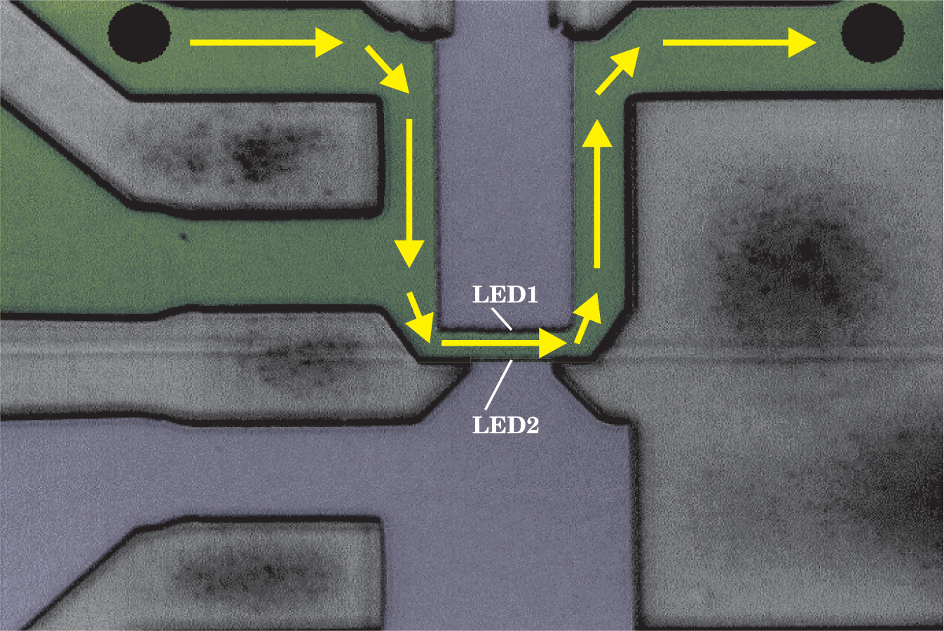
Wunderlich and Kästner realized they could observe the spin Hall effect by reconfiguring an LED. In their device, a p-doped channel lies above n-doped material, but not directly above. When spin-polarized holes accumulate at the edges of the channel, they recombine with electrons that jump up and sideways from the n-doped material to meet them. The resulting circularly polarized light originates from the edges of the LED. The chip-like device is shown in figure 3.

Figure 3. The Hitachi experiment exploits a chiplike device made from p-doped GaAs (green area) on top of n-doped GaAs (blue area). When an electric field is applied across the p-doped material, holes flow (yellow arrows) between the two terminals (black circles). The spin Hall effect is detected by either or both of the two LEDs when electrons from the n-doped GaAs recombine with spin-polarized holes that accumulate at the edges of the central 1.5-μm-wide p-doped channel.
(Adapted from ref. 6.)
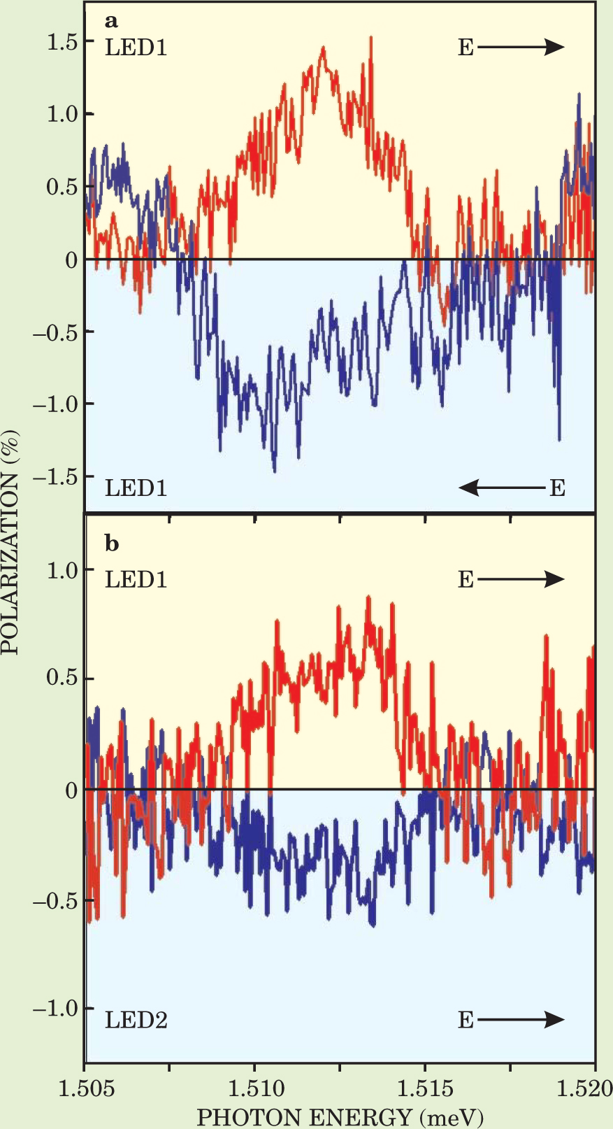
LEDs, including the novel Hitachi device, emit a spectrum of light with several peaks. Careful calibration identified the appropriate peak (at 1.512 meV in the experiment).
The results appear in figure 4. As expected, when the direction of the electric field is reversed, the polarization signal at one edge switches sign (top panels). And just as expected, when the field direction stays the same, the polarization at the two edges is opposite (bottom panels).

Figure 4. The light emitted by the Hitachi LEDs at a photon energy of 1.510 to 1.515 meV comes from the recombination of spin-polarized holes and electrons. The direction of the polarization reverses with the applied electric field (a) and is opposite at the two edges (b).
(Adapted from ref. 6.)
Weak and strong coupling
Spin–orbit coupling, the key ingredient of the spin Hall effect, originates from Paul Dirac’s famous union of special relativity and quantum mechanics. In 1929, two years after Dirac’s theory appeared, Nevill Mott applied it to the problem of scattering spinning electrons off atoms. 7 Roughly speaking, as an electron swings by an atom, it sees an effective magnetic field –(v/c) × E due to the atom’s Coulomb field. The coupling of an electron’s spin to the magnetic field sends spin-up electrons one way and spin-down electrons the other. This “skew scattering” as Mott termed it, is used to produce spin-polarized particle beams at accelerators.
In Dyakonov and Perel’s extrinsic theory, impurities serve as skew scatterers. In the intrinsic theories, spin–orbit coupling of electrons to the lattice atoms acts with the applied electric field to change the band structure. As a result, the electrons’ group velocity acquires a spin-dependent transverse component that leads to a transverse spin current.
The stronger the spin–orbit coupling, the stronger the spin Hall effect. For semiconductors, that means heavier atoms with their larger Coulomb potentials are better than light atoms. In addition, valence-band electrons, which occupy p-like states, have far stronger coupling than conduction band electrons, which occupy s-like states.
A further boost to the coupling comes from breaking the up–down symmetry of the lattice. Silicon has inversion symmetry, but GaAs does not. Confining the charge carriers in a thin layer with a strong electric field also breaks up–down symmetry and strengthens the coupling.
In the Santa Barbara experiment, the spins belong to conduction-band electrons whose spin–orbit coupling to the atoms of the GaAs lattice is weak despite the lack of inversion symmetry. Here, the spin Hall effect most likely originates extrinsically from skew scattering off impurities, rather than intrinsically from the GaAs lattice. The Santa Barbara team checked this hypothesis by repeating their experiment on a strained sample. If the effect originated in the lattice, then it should depend on the strain direction. It doesn’t.
The charge carriers in the Hitachi experiment are holes whose already strong coupling to the GaAs lattice is increased by their confinement in a narrow layer. Having measured the impurity concentration in their sample, the Hitachi researchers believe it to be too low to account for the polarization they observe. The spin Hall effect in their sample is, they believe, intrinsic in origin.
The controversy surrounding the intrinsic effect doesn’t stem from the effect itself, but from what happens when impurities are present. When the electric field is switched on, the spins polarize and head off to different edges of the strip. In the absence of impurities, the electrons would continue to accelerate down the strip, but in a real, impurity-ridden lattice, the electrons must decelerate to stabilize the current, either by scattering off impurities or by slamming against the sample boundary. And when the electrons decelerate, the intrinsic effect reverses direction and could, in principle, cancel itself out.
In some models, the steady acceleration caused by the field doesn’t necessarily cancel the abrupt deceleration that occurs when electrons slam head-on into a few sparsely distributed impurities. But in other models, the cancellation is exact and, in some cases, originates from the lattice as well as impurities.
Even the notion of a spin current is somewhat problematic. As an electron travels through the bulk to reach the edge, its charge remains the same. But its spin, thanks to spin–orbit coupling, is not conserved. Relating spin accumulation observed at the edges to a spin current through the bulk is not straightforward.
Sankar Das Sarma of the University of Maryland in College Park has been closely following the controversy as its unfolds. “The theoretical situation is a complete mess,” he says.
References
1. M. I. Dyakonov, V. I. Perel, JETP Lett. 13, 467 (1971)
Phys. Lett. A 35, 459 (1971) https://doi.org/10.1016/0375-9601(71)90196-4 .2. J. Hirsch, Phys. Rev. Lett. 83, 1834 (1999) https://doi.org/10.1103/PhysRevLett.83.1834 .
3. S. Murakami, N. Nagaosa, S. C. Zhang, Science 301, 1348 (2003) https://doi.org/10.1126/science.1087128 .
4. J. Sinova, D. Culcer, Q. Niu, N. A. Sinitsyn, T. Jungwirth, A. H. MacDonald, Phys. Rev. Lett. 92, 126603 (2004) https://doi.org/10.1103/PhysRevLett.92.126603 .
5. Y. K. Kato, R. C. Myers, A. C. Gossard, D. D. Awschalom, Science 306, 1910 (2004) https://doi.org/10.1126/science.1105514 .
6. J. Wunderlich, B. Kästner, J. Sinova, T. Jungwirth, Phys. Rev. Lett. (in press).
7. N. F. Mott, Proc. R. Soc. London A 124, 425 (1929) https://doi.org/10.1098/rspa.1929.0127 .


