Sandia heads up new nanoengineering institute
DOI: 10.1063/1.2812117

“Engineering is changing incredibly rapidly, and engineering education must change in major ways in response,” says Paul Peercy, dean of engineering at the University of Wisconsin–Madison. “The boundaries between science and engineering are fading. Thirty or forty years ago, people worked alone and in small teams. If you think about the next generation of solutions to complex problems, they’re going to be obtained by large interdisciplinary teams.”
Forging the mindset and connections to nurture large interdisciplinary teams is the aim of the National Institute for Nano-Engineering, a partnership among industry, government, and university researchers that is getting started with the Department of Energy’s (DOE’s) Sandia National Laboratories in New Mexico as its base. Besides Sandia, 12 universities and 7 companies make up NINE’s founding members, but the partnership is open to expansion, and researchers from any university can participate, says Duane Dimos, Sandia’s director of materials science and engineering. NINE’s main focus is on undergraduate and graduate students, including developing curricula in nanoscience and nanoengineering that will be both used within NINE and shared openly with academic institutions. “NINE will impedance match to broker internships with industry and collaborations with Sandia,” says Paul Fleury, Yale University’s dean of engineering.
Hundreds of students
Dimos points to institutes in Europe, Singapore, and South Korea as models for NINE, singling out the 23-year-old IMEC—the Interuniversity MicroElectronics Center in Belgium. In microelectronics and nanoelectronics, he says, “IMEC has become a strong player throughout Europe, and it has a large industrial component. By combining what they do at the center with what they do at their home universities, students are getting a really interesting education. We are emulating that, although we will add our own twist in that universities might be more active in driving the program [at NINE].”
Many practical matters are still being worked out, says Dimos. “We anticipate having a central facility in Albuquerque next to the Sandia campus.” Participating researchers would work at both Sandia and partner institutions, and they would have access to equipment at Sandia, such as the Microsystems and Engineering Sciences Applications facility (see Physics Today, October 1999, page 65 ).
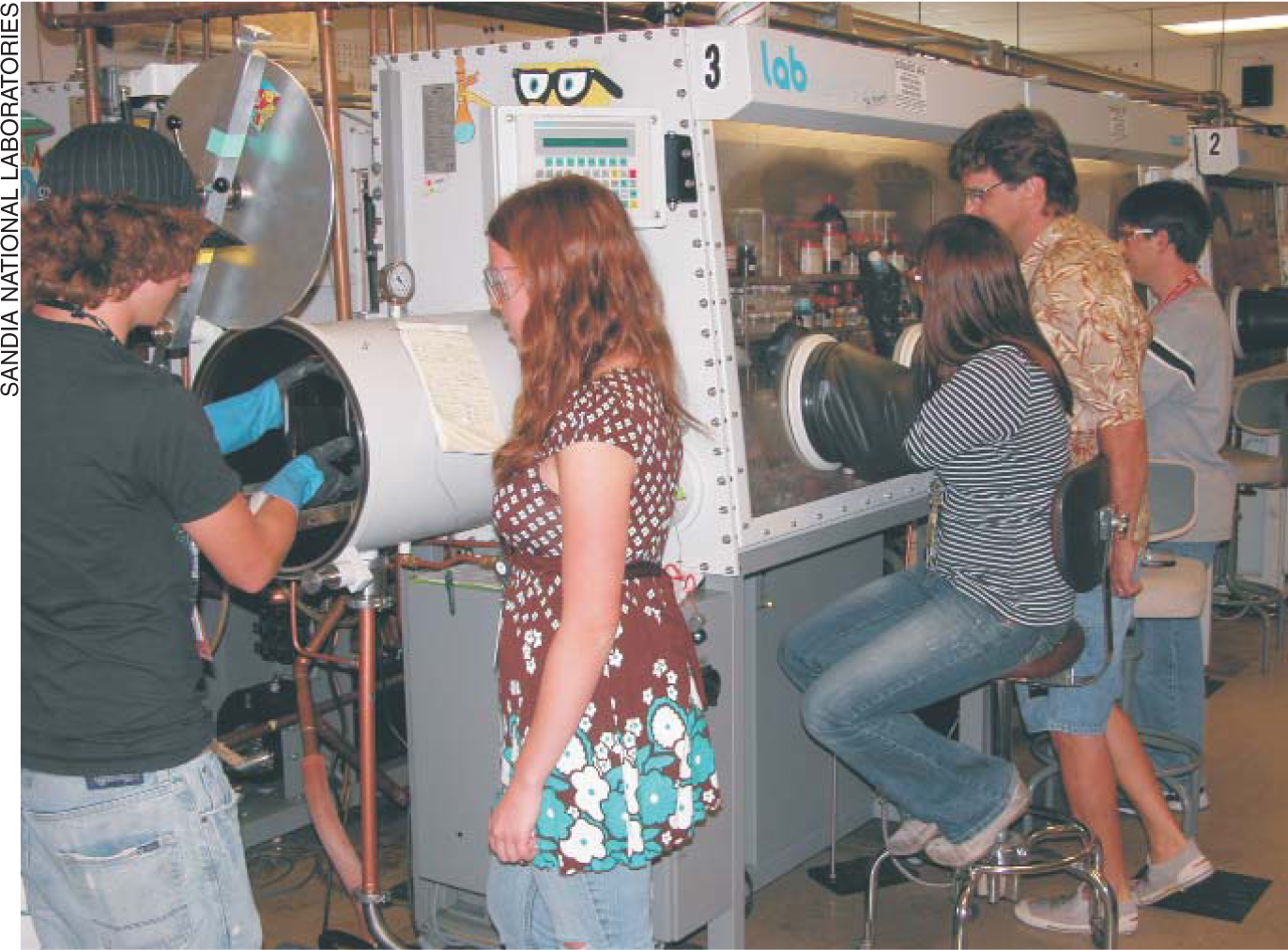
The institute kicked off this past July with a two-week workshop at Sandia attended by three dozen undergraduate and graduate students. Some 13 projects are under way in topics such as nanowire electronics, flow and rheology of nanomaterials, catalytic function of nanomaterials, and manipulation of nanowires, Dimos says. The goal, he adds, is to eventually involve a couple hundred undergrads and a similar number of graduate students.
Industrial guidance
“There is a strong belief at Corning that education is falling short of expectations,” says Daniel Ricoult, the company’s director of technology assessment. “That’s why when we heard about the concept of NINE, we were intrigued. It’s a nice way to build bridges between industry and academia.”
Sharon Smith, who leads Lockheed Martin Corp’s efforts in nanotechnology, agrees: “We have to have a really good pipeline of talented scientists and engineers, and we see NINE as an exciting program that will benefit us in the future.” Her company, she adds, hires 5% of new engineering bachelor’s recipients in the US each year.
“We see nanotechnology as a key area,” Smith says, “because it’s going to impact virtually every aspect of our business.” New materials are lighter and stronger and have new capabilities, she adds, citing as applications multifunctional materials, embedded sensors, and energy. “We have no lack of problems to be solved.”
NINE’s industrial partners will provide guidance on the technical directions of research, Smith adds. “We will be looking for areas of research that will benefit our industry as a whole, and we will be looking to provide a unique experience for students to learn how what they do in the NINE program could benefit industry.” As part of the collaboration, she adds, NINE partners are working on an overarching agreement on how to handle intellectual property “with the understanding that there may be cases for which the agreement has to be altered.”
Sandia has jump-started NINE with $7.5 million for collaborative research projects. The institute needs funds for a central building plus an annual budget on the order of tens of millions of dollars to pay for research, travel, and curriculum development, Fleury says. Industrial partners may contribute funding, although that is not part of the current agreement. Rather, NINE coordinators have their hopes pinned on applying to DOE for funding as one of the Discovery Science and Engineering Innovation Institutes outlined in the America Creating Opportunities to Meaningfully Promote Excellence in Technology, Education, and Science Act. The COMPETES Act was signed by President Bush on 9 August (see Physics Today, September 2007, page 34 ), but it’s too early to say which aspects of it will ultimately be funded.
Founding NINE partners
The founding partners of the National Institute for Nano-Engineering are Sandia National Laboratories; Corning Inc; Exxon Mobil Corp; IBM; Intel Corp; Goodyear Tire and Rubber Co; Lockheed Martin Corp; Procter and Gamble; Harvard University; Harvey Mudd College; Rensselaer Polytechnic Institute; Rice University; University of California, Davis; University of Florida, Gainesville; University of Illinois at Urbana-Champaign; University of New Mexico; University of Notre Dame; University of Texas at Austin; University of Wisconsin–Madison; and Yale University.

Students learned to synthesize nanoparticles this past summer at the kickoff workshop of the National Institute for Nano-Engineering at Sandia National Laboratories.
SANDIA NATIONAL LABORATORIES
More about the authors
Toni Feder, American Center for Physics, One Physics Ellipse, College Park, Maryland 20740-3842 US . tfeder@aip.org


