Phonon spectrometry goes nanoscale
DOI: 10.1063/PT.3.2262
Nanostructures often appear to play by a different set of rules from those governing bulk materials. Mechanically, they tend to be stronger, more ductile, and more flexible than their bulk counterparts (see Physics Today, November 2013, page 14 ). Shrinking a material’s scale can also change its thermal properties. In a bulk semiconductor or insulator, for instance, those properties are primarily determined by phonon–phonon and phonon–defect interactions; in nanostructures, phonon–surface interactions dominate.
A precise description of phonon–surface interactions has proven difficult to pin down from first principles. It’s generally agreed that phonons with wavelengths much larger than a surface’s characteristic roughness length scale should reflect specularly, like light off a smooth mirror, and that those with wavelengths much shorter than the roughness length scale should scatter diffusively. Theories differ, however, as to what happens at intermediate wavelengths.
Richard Robinson and coworkers at Cornell University have introduced a tool that could shed new light on the problem: a microscale phonon spectrometer. 1 The device, pictured in the figure, uses superconducting tunnel junctions (STJs) cooled to a fraction of a kelvin to detect the frequency dependence of phonon transmission through silicon nanosheets.

The spectrometer shown in this false-color scanning electron microscope image detects the transmission of phonons through an array of silicon nanosheets etched out of a raised mesa. Phonons generated by a source superconducting tunnel junction (STJ) are detected by the current they produce as they strike two detector STJs. To ensure a direct path between the source and the phonon-absorbing tip of the detectors, those elements were built facing each other, along the inclined edges of the 800-nm-tall mesa, as depicted in the inset. (Adapted from ref.
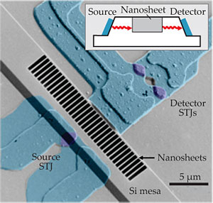
One STJ serves as the phonon source. When a current is driven through the junction at a sufficiently large bias that the electron energy eV exceeds twice the energy Δ of the superconducting gap, the tunneled electrons shed excess energy in the form of phonons. The resulting phonon energy distribution is broad and uniform, with a sharp cutoff at eV − 2Δ. To probe just a narrow slice of spectrum, the researchers modulate the bias voltage: The change in the phonon energy distribution due to such modulation is concentrated in a narrow band near the cutoff energy.
Phonons that pass through the nanosheets strike a superconducting film that’s connected to a pair of additional STJs, the detectors. The incoming phonons excite Cooper-paired electrons, which give rise to a detectable tunneling current. (The detector STJs are configured as a superconducting quantum interference device, so that Josephson currents, which might otherwise mask the phonon-induced current, can be suppressed with an applied magnetic field.) By monitoring the ratio between the detector and source currents, the researchers can tease out the wavelength dependence of phonon transmission.
Just because a phonon passed through a nanosheet, however, doesn’t mean it didn’t scatter along the way. Some scattered phonons eventually find their way to the detector. But others scatter backward, exit the way they entered, and escape into the environment undetected. Using a theoretical model that incorporates Monte Carlo simulations of phonon trajectories, the researchers could relate the phonon transmission rate to the effective scattering mean free path.
Although the tunnel-junction technique for phonon spectrometry was developed more than four decades ago, 2 it has until now been used exclusively on bulk materials. Applying the technique to nanostructures required more than simply miniaturizing the spectrometer’s individual elements; arrangement is also important. To ensure that phonons have a direct path between the source and the detector, those two elements should face each other, with the nanosheets aligned between them. That’s difficult to achieve with standard nanofabrication techniques, which require STJs to lay face-flat against an underlying substrate.
The Cornell team’s solution was to incorporate a 7-µm-wide raised mesa into the substrate surface. The source STJ and the phonon-absorbing tip of the detector were deposited along the mesa’s steep edges, as depicted in the figure’s inset. Nanosheets of varying thickness and length could then be etched out of the mesa itself. “It’s a great idea,” says Olivier Bourgeois, of the Néel Institute in Grenoble, France. “And in terms of nanofabrication, it’s extremely difficult to execute.”
Early spectroscopic studies using arrays of 100-nm-thick sheets produced a surprise result. The etching process creates sheets with a characteristic surface roughness of 1 nm. But even for phonon emissions with peak wavelengths in the 10- to 15-nm range, transmission through the sheets was consistent with diffusive scattering. That would mean the standard theory of phonon scattering, which predicts mostly specular reflection at those wavelengths, may overestimate the sheets’ thermal conductivity.
Follow the phonons
The extent to which one can alter a material’s thermal properties by tinkering with its surface structure isn’t yet fully known. In 2008, a team from the University of California, Berkeley, led by Arun Majumdar and Peidong Yang, reported experiments showing that surface roughening could reduce the room-temperature thermal conductivity of silicon nanowires more than fivefold, to around 1/100 the conductivity of bulk silicon. 3 That would make them attractive for heat-harvesting thermoelectric devices, where the ideal material can simultaneously conduct electrons and maintain large temperature gradients.
It was never clear, however, what physical mechanisms underlay the Berkeley results. Presumably, roughening the walls slows transport by extending the diffusive-scattering regime to longer phonon wavelengths. But even perfectly diffusive scattering at all wavelengths wouldn’t fully explain the precipitous drop. Phonon spectrometry could provide a more rigorous way to probe and quantify the behavior.
The Cornell team’s approach may also aid the development of nascent applications such as phononic logic circuits and frequency-selective transport via phonon echo chambers. “Right now, one of my grad students is making nanoholes in the mesas and trying to come up with spacings that would give rise to phononic crystal effects,” says Robinson. “Now that we can fabricate a microscale phonon spectrometer, we can explore questions that were previously inaccessible.”
References
1. J. B. Hertzberg et al., Nano Lett. (in press).https://doi.org/10.1021/nl402701a
2. W. Eisenmenger, A. H. Dayem, Phys. Rev. Lett. 18, 125 (1967); https://doi.org/10.1103/PhysRevLett.18.125
H. Kinder, Phys. Rev. Lett. 28, 1564 (1972). https://doi.org/10.1103/PhysRevLett.28.15643. A. I. Hochbaum et al., Nature 451, 163 (2008). https://doi.org/10.1038/nature06381


