NSF reconfigures nanoscience network
DOI: 10.1063/PT.3.2976

In September NSF awarded $81 million over five years to 16 institutions. The National Nanotechnology Coordinated Infrastructure (NNCI) is a continuation of NSF’s efforts in support of the National Nanotechnology Initiative.
The 16 winning institutions are located in 15 states. Half of them were part of NSF’s previous nanoscience network and half are newcomers; many have teamed up with partner institutions. (A list of NNCI sites is available at http://www.nsf.gov/news/news_summ.jsp?cntn_id=136211 .)
The awards, which range from $500 000 to $1.6 million annually, are to facilitate serving external users. The money will go for hiring staff, upgrading equipment, subsidizing user fees, performing educational outreach, developing sample protocols, and the like. By the end of the year, NSF will select one of the 16 sites to act as NNCI coordinator “to enhance impact as a national infrastructure network of user facility sites,” says NSF senior engineering adviser Lawrence Goldberg.
Multiscale tools
The Cornell NanoScale Science and Technology Facility, a continuing NSF site, has nanometer- to centimeter-scale fabrication tools, including for electron-beam lithography, photolithography, nano-imprint lithography, and direct-write processes. Visitors come, for example, to make x-ray optics with features 5–10 nm wide, says site director Daniel Ralph. “We also have sophisticated optical lithography—people make biocompatible fluidic channels to view blood vessels.”
To access the Cornell nanofacility, researchers submit a description of the work they want to do. The center staff checks for technical feasibility and materials compatibility. “There is no judgment in terms of merit,” says Ralph. “As long as a project is feasible with our toolset, we try to get you in within two weeks.” At any given time, several hundred projects are in progress. Users don’t need experience, he says. “We can help design processes. We offer more hand-holding and can be more flexible about materials than industrial foundries.”
The Kentucky Multi-scale Manufacturing and Nano Integration Node, a partnership between the Universities of Louisville and Kentucky, is new in the NSF network. “This is a huge opportunity for us,” says principal investigator Kevin Walsh of Louisville. “It’s going to get the word out.”
The word is that the Kentucky nanocenter offers facilities ranging from a $30 million, 10 000-square-foot clean room to three-dimensional printers that use two-photon deposition methods to make things with roughly 100-nm resolution. “We can cater to people who are interested in making meso and macro products with embedded micro and nano features,” says Walsh. “When people visit, they are blown away. They can’t imagine such facilities in a state known for horses and the Kentucky Derby.”
A potential application could be personalizing a bone replacement. “In the future, you will do an MRI, do reverse engineering, 3D print a custom bone, and embed wireless microsensors for feedback and tiny reservoirs for drug delivery so the body will not reject the bone,” says Walsh.
Besides forming new collaborations and putting facilities to more use—those at the Kentucky center are now at about half capacity—another benefit of being part of the NSF network, says Walsh, “is that the [host] university sees the recognition, and continues to invest in the field, continues to hire people. It’s a catalyst.”
“Collaborations on steroids”
“A lot of toxins that travel the planet are nano,” says Michael Hochella, director of the Virginia Tech National Center for Earth and Environmental Nanotechnology Infrastructure, also a newcomer to the NSF network. Global warming, pollution, and disease transmission are among the things the center is set up to study.

Michael Hochella readies his airplane for a flight over a contaminated mine site in Montana. He occasionally flies other researchers to visit remote locations or to get aerial views for their studies of, for example, the spread of toxic nanoparticles.
MICKY GUNTER, UNIVERSITY OF IDAHO

“Geo and environmental sciences have been the small kids on the block in terms of nanoscience and money in the field,” he says. Being named an NSF center is “a huge boost for our field, not just for Virginia Tech. It creates a beehive of activity. The contacts will put our collaborations on steroids.”
The center’s facilities include transmission electron microscopes and atmospheric chambers for growing nanomaterials to mimic things found in nature. “We have over 21 000 square feet of instrumentation and laboratory space,” says Hochella. “We go out and collect nanomaterials in nature to see how they work. They are in lakes, air, soil, really everywhere.”
Hochella is keen to recruit minority scientists, who are “grossly underrepresented” in Earth sciences. “Being an NSF nanohub will be a good attractor,” he says. “And we have a good chunk of our budget for bringing underrepresented researchers—all expenses paid—here. It will be a very aggressive program.”
Stanford University, a repeat member in the NSF network, offers tools in areas from electronics to Earth sciences and serves more than 1000 external users a year. A new emphasis, says site director Kam Moler, is keeping track of sample preparation and instrument protocols in a “living document.”

Electrical engineering graduate student Marjan Aslani loads a silicon wafer into an electron-beam lithography system as Kam Moler, site director of the Stanford University nanocenter, looks on. The system can etch features down to about 10 nm.
UNIVERSITY HUMAN RESOURCES, STANFORD UNIVERSITY
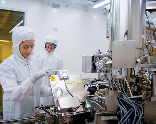
“If you want to make something out of silicon, you can buy a textbook or hire an expert. But there are many quirky materials, like mercury telluride heterostructures,” Moler says. “There is a big gap between what goes in peer-reviewed publications and what is in somebody’s lab notebook.
“I want to make the knowledge base more formal, more flexible, and more on-demand. I have 73 faculty members who have agreed to encourage their students to write up protocols to share. How they make devices, how they do processing,” says Moler. “We are hoping to map out a web of knowledge for how to be the most fantastic e-beam lithographer,” she says. “And eventually, we hope everything in all the nanofacilities will be covered.”
Site competition
Unlike previous NSF award competitions, in which institutions joined up and applied as networks, this time they applied individually or in small regional teams. “We wanted to open up the competition more broadly,” says NSF’s Goldberg.
The competition was divided into groups from the eastern, western, and central US. “We were seeking geographically distributed sites with diverse and complementary facilities,” Goldberg says. Before settling on that format, NSF had conducted and then scrapped a competition for networks. That led to a tight schedule, and with funds from fiscal year 2015 to award, he says, the evaluators convened at NSF headquarters for “reverse site visits” via the Web instead of actually visiting the sites.
More about the authors
Toni Feder, tfeder@aip.org


