New All-Electrical Measurement Schemes Can Detect the Spin State of a Single Electron
DOI: 10.1063/1.1825260

The basic steps of quantum information processing are relatively straightforward, at least on paper: Prepare qubits in an appropriate initial state, let them evolve under the influence of one- and two-qubit gate operations, and read out the results. But obtaining scalable physical implementations of these steps continues to challenge researchers, in part because of the conflicting requirements of ensuring sufficient isolation from the environment to maintain qubit coherence and allowing sufficient coupling between qubits to enable the requisite two-qubit operations.
Spins in semiconductors have many desirable properties that make them candidates for quantum information implementations. 1 The spins can have very long coherence times, and an extensive repertoire of fabrication expertise, amassed over decades, can be exploited for sample preparation. Such properties have also raised hopes for spintronics—exploiting the spin degree of freedom in addition to the charge degree of freedom in electronic circuits. Spintronics, too, will require the ability to controllably generate, manipulate, and detect spins in the solid state.
Most studies of semiconductor spins—at least in gallium arsenide—have relied on optical techniques for creating, manipulating, and detecting the spin states (see the article by David Awschalom and Jay Kikkawa in Physics Today, June 1999, page 33 ). And recently, using magnetic resonance force microscopy, Dan Rugar and colleagues have demonstrated mechanical location of a single spin (see Physics Today, September 2004, page 21 ).
Now come two reports of all-electrical measurements of spin states in semiconductors. At Delft University of Technology in the Netherlands, a team of researchers led by Leo Kouwen-hoven has used a quantum point contact to make single-shot measurements of individual electron spins in a quantum dot. 2 A group led by Hong-Wen Jiang and Eli Yablonovitch at UCLA has detected spin-resonance-induced spin flips of single electrons in a field-effect transistor. 3
A single-shot spin measurement
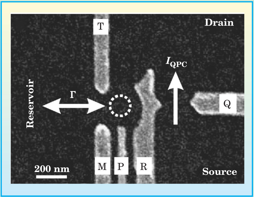
Advances in quantum-dot fabrication over the past several years now allow exquisite control over such “artificial atom” systems. Making dots that contain a controlled number of excess electrons—even just one—is now almost routine. In the GaAs quantum dot used by the Delft group (see figure 1), the spacing between the dot’s energy levels is so large that the only level that can be occupied is the dot’s ground state. Furthermore, Coulombic repulsion ensures that at most one electron will occupy that level. An applied magnetic field of 10 tesla lifts the degeneracy between the spin-up and spin-down ground-state levels by an amount larger than the thermal energy at the experiment’s temperature of 300 mK.

Scanning electron micrograph of a semiconductor device for electrical detection of an electron’s spin state. Voltages applied to the lettered electrodes define a quantum dot (dashed circle) next to a quantum point contact (constriction on the right). The current I QPC through the quantum point contact is sensitive to the charge state of the dot, and can be monitored to detect when an electron tunnels between the dot and the reservoir.
(Adapted from ref. 2.)
Careful manipulation of the dot’s energy levels is a key component of the spin-state detection scheme. The scheme consists of two parts: mapping the spin state to a charge state and measuring the charge state. Figure 2(a) shows the sequence of voltages applied to a gate electrode near the dot that shifts the dot’s energy levels. With no gate voltage applied, the spin-up and spin-down energies are above the Fermi level of the reservoir, E F, and the dot is empty. A sufficiently large voltage applied to the gate electrode will lower the ground-state energy levels below E F, and a single electron can enter the dot in either spin state.

Detecting the spin state of a single electron. (a) When a large voltage V P is applied to gate P, the potential of the quantum dot is lowered and a single electron is injected into the dot. When the voltage is then reduced to a carefully determined intermediate value, the electron on the dot can leave only if its spin is down. (b) The charge state of the quantum dot can be monitored with the current through the adjacent quantum point contact. The current is sensitive to V P and also to the number of electrons in the dot. A spin-up electron that enters the dot in the injection stage can leave only when the dot is emptied. A spin-down electron, whose energy is higher by the Zeeman splitting, can leave in the read-out stage. After it leaves, a spin-up electron can enter the dot. These transitions produce a detectable current pulse through the point contact. The red lines indicate the threshold level used to determine whether a current pulse occurs during the read-out stage.
(Adapted from ref. 2.)
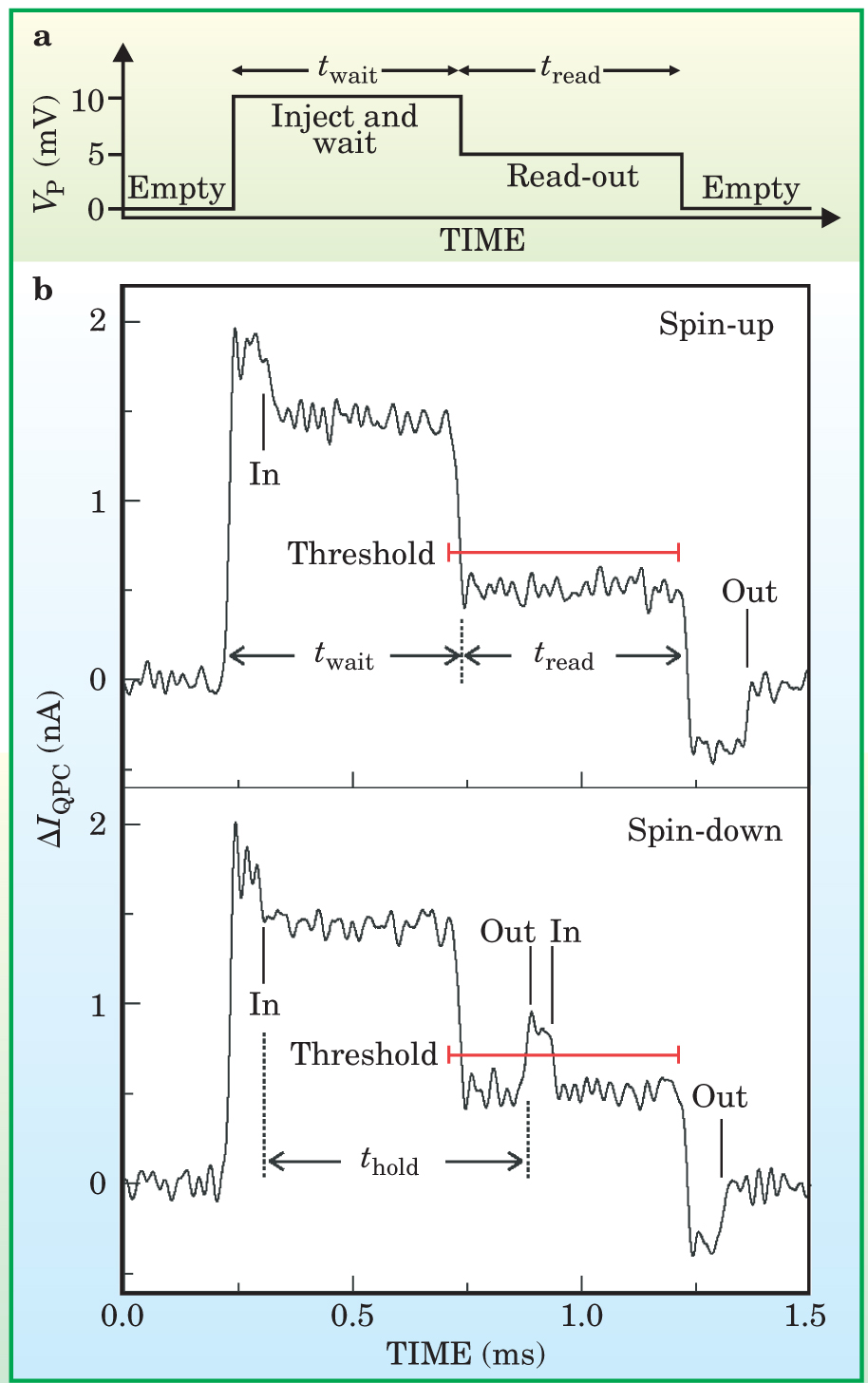
The heart of the spin-to-charge conversion is the next step: raising the dot’s energy so that E F falls between the dot’s Zeeman levels. At that bias, an electron in the lower-energy spin-up state must remain in the dot, but it’s energetically favorable for a spin-down electron to leave the dot. Once empty the dot can receive a replacement, spin-up electron from the reservoir.
The Delft group detected changes in the charge state of the dot using an adjacent quantum point contact, which serves as a sensitive electrometer. The presence of a single electron in the dot is sufficient to induce a measurable change in the point contact’s conductance. Thus, as shown in figure
Spin flips, thermal fluctuations, and slow tunneling rates are among the sources of error that can affect the accuracy of the spin determination. Through careful examination and calibration of such errors, the Delft group was able to obtain an accuracy of 65% for unaveraged, single-shot measurements. The group is currently working to improve that figure of merit.
“Before, it was not possible to measure electrically the state of a single spin in the solid state,” says David DiVincenzo of IBM’s T. J. Watson Research Center. “Now it can be done.”
Single-spin resonance detection
The UCLA team used a different device for their work: a field-effect transistor in a commercial silicon integrated circuit. By using a paramagnetic trap located near the conduction channel in the FET (see figure 3), the researchers demonstrated electrical detection of single-electron spin flips induced by magnetic resonance.

A paramagnetic trap in a field-effect transistor can produce a measurable change in the FET current due to its influence on the two-dimensional conduction channel between the source and drain electrodes.
(Adapted from ref. 3.)
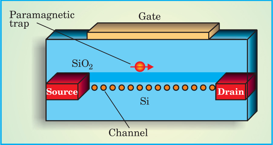
The channels in today’s FETs are so small, and the production technology so developed, that it’s rare to find defects near FET conduction channels. But the UCLA researchers were able to introduce a single defect by applying a voltage spike to the FET gate electrode. Using the modified FET, the team was able to sense the spin orientation of electrons in the trap.
In the UCLA experiment, the two available states of the trap were with one or two electrons in it. The “empty” state corresponded to a single electron, either spin-up or spin-down. By the Pauli principle, a second electron could hop onto the defect—switching the trap to the “filled” state—only if it has the opposite spin to the first electron.
The UCLA measurement scheme bears many similarities to that used by the Delft group. An applied magnetic field lifts the spin-state degeneracy for the trap’s second electron, and the system is biased so that the Fermi level of the FET’s conduction channel falls between the spin-up and spin-down energy levels. If the first electron in the trap is in the lower-energy, spin-up state, the trap remains singly occupied. But if the first electron is in the higher, spin-down state, a second electron can hop from the conduction channel onto the trap. The presence of a second electron on the defect site decreases the current through the conduction channel; like the Delft group’s quantum point contact, the FET thus functions as a sensitive electrometer.
The current through the FET shows random switching between two values (see figure 4(a)) as electrons hop onto and off the defect site. But by plotting a histogram of the current values (figure

Electrical monitoring of the trap’s spin state with a field-effect transistor. (a) An electron hopping on and off the paramagnetic trap in the FET produces a so-called random telegraph signal as the current jumps between two values. (b) A histogram of the current values shows two peaks, which correspond to the trap’s being empty (large peak) and filled (small peak). (c) In electron spin resonance, microwave radiation that’s resonant with the Zeeman splitting of the electron in the trap can modify the likelihood that the trap is occupied. The resonance here occurs at a field of 1.602 T.
(Adapted from ref. 3.)
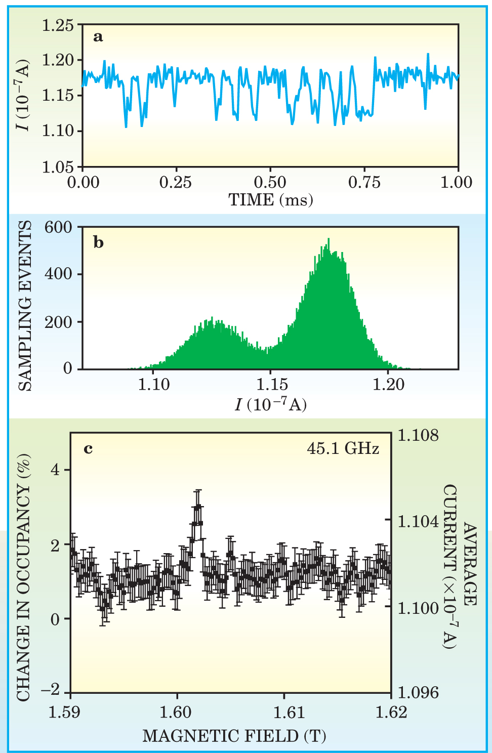
In an electron spin resonance setup, the UCLA team used microwaves to flip the spin state of the singly occupied trap. When the radiation was resonant with the trap’s Zeeman splitting, the occupation probabilities for being in the singly and double charged states changed, as shown in figure
Toward full control
These developments join several other recent advances in electrical control of semiconductor spins. Awschalom and co-workers at the University of California, Santa Barbara, have shown that modulation of the electron’s Landé g factor and strain can be exploited for coherent electrical manipulation of spins. 4 And Harvard University’s Charles Marcus and colleagues have demonstrated electrically controlled coupling between spins in quantum dots. 5
The ability to control spins electrically would offer several advantages. In particular, devices could be self-contained on a chip without the need for lasers and optical tables. And electrical implementations could interface naturally with conventional electronic circuits.
References
1. D. Loss, D. P. DiVincenzo, Phys. Rev. A 57, 120 (1998).https://doi.org/10.1103/PhysRevA.57.120
2. J. M. Elzerman, R. Hanson, L. H. Willems van Beveren, B. Witkamp, L. M. K. Vandersypen, L. P. Kouwen-Hoven, Nature 430, 431 (2004).https://doi.org/10.1038/nature02693
3. M. Xiao, I. Martin, E. Yablonovitch, H. W. Jiang, Nature 430, 435 (2004).https://doi.org/10.1038/nature02727
4. Y. Kato et al., Nature 427, 50 (2004);https://doi.org/10.1038/nature02202
Y. Kato et al., Science 299, 1201 (2003).https://doi.org/10.1126/science.10808805. N. J. Craig et al., Science 304, 565 (2004).https://doi.org/10.1126/science.1095452
More about the authors
Richard J. Fitzgerald, rfitzger@aip.org


