Makers of quantum dots share Nobel Prize in Chemistry
DOI: 10.1063/PT.3.5356

An LED’s color depends on the semiconductor material it’s made of. When current flows through an LED, an excited electron crosses the semiconductor bandgap. It can then relax and recombine with a hole in the valence band, resulting in the emission of a photon. The light’s color, therefore, varies with the energy required to cross the bandgap. (To learn more about blue LEDs, see Physics Today, December 2014, page 14 .)
But new behavior emerges when a semiconductor shrinks to a few nanometers in size. When electrons in nanocrystals get excited, the emitted photons can have only certain allowed energies. And as the space that an electron can occupy shrinks, so too do the allowed values of its wavelength, according to the particle-in-a-box model in quantum mechanics, and the bandgap of the semiconductor widens.
Semiconductor nanocrystals are often called quantum dots, and the wavelengths they shine at depend only on their size: Bigger quantum dots emit red and orange light, and smaller ones shine green and blue. (See the article by Dan Gammon and Duncan Steel, Physics Today, October 2002, page 36 .)
For discovering quantum dots and for developing a reliable, high-quality method to manufacture them, Aleksey Yekimov of Nanocrystals Technology Inc. in New York, Louis Brus of Columbia University, and Moungi Bawendi of MIT were awarded this year’s Nobel Prize in Chemistry. Their contributions to the field have helped lead to all sorts of technological applications, such as quantum-dot-based TVs available for purchase today, medical-imaging technology, and highly efficient IR detectors.

Aleksey Yekimov
NEXDOT

Louis Brus
COLUMBIA UNIVERSITY

Moungi Bawendi
JUSTIN KNIGHT/MIT
Frozen in glass
Since medieval times, glassmakers have known that adding small amounts of powdered metal-oxide impurities to a molten mixture of sand and ash would yield various colors of glass when cooled. But what wasn’t known was why it worked. Hundreds of years later emerged the interdisciplinary field of colloid science, which focuses on the study of small solid or liquid particles mixed and suspended in a solution. But the exact mechanism that produces color in stained glass remained uncertain until the early 1980s.
Yekimov wanted to learn more about the growth of colloids in stained glass, so he began studying them at the S. I. Vavilov State Optical Institute in Leningrad in the Soviet Union. He and his PhD mentee, Alexei Onushchenko, tinted silicate glass with a single type of semiconductor colloid—in their case, a little bit of copper chloride—and measured the glass’s optical absorption.
Based on the absorption measurements, they inferred that small CuCl crystals were forming in the molten glass solution. Variations in temperature regulated the size of the CuCl crystals, and subsequent x-ray scattering measurements showed that the crystals ranged from just a few nanometers to tens of nanometers in size. Yekimov and Onushchenko also observed that the smaller nanocrystals emit shorter wavelengths of light, whereas larger ones have longer wavelengths. 1
Yekimov correctly identified in 1981 that quantum confinement effects are responsible for the changing wavelengths of light. Sufficiently energetic electrons can jump across the material’s bandgap to the conduction band. When the electrons are electrostatically attracted to the holes left in the valence band, they combine. In doing so, they emit photons at a specific wavelength, and for nanocrystals, that wavelength is limited by the 3D confinement of the electrons.
Shortly after Yekimov’s discovery, he began collaborating with a theoretician named Alexander Efros, who was based at the Ioffe Institute in Leningrad and is now at the US Naval Research Laboratory. They further studied the size-dependent optical and electronic properties of various semiconductor nanocrystals, but they faced a challenge. The nanocrystals were frozen in glass, so the researchers had limited opportunities to manipulate or change them further.
“One day I was called into the special department of the Ioffe Institute,” says Efros, “where the chief of the department said, ‘Do you know Louis Brus? Who is Louis Brus?’ He gave me an open envelope, which was a preprint of a journal that the Ioffe Institute didn’t have.” Inside was a copy of a 1983 paper that Brus had recently published. 2 (He had found a translated copy of Yekimov’s first paper and was intrigued.) “We learned that some people on the other edge of the world are working on the same topic,” says Efros, “and it was very exciting for us.”
In liquid
The Cold War had prevented most exchanges between Soviet and US scientists. So unbeknownst to Yekimov and Efros, Brus had also been researching quantum dots, at Bell Labs in Murray Hill, New Jersey. He was preparing nanometer-sized cadmium sulfide crystals by precipitating them out of a liquid that was injected with precursor ions. He observed that over time, the CdS crystals dissolved and then recrystallized to larger sizes, with the aged ones reaching a diameter of up to 12 nm.
“The initial observation was accidental,” says Brus. “I tried to figure out what it meant, and it took a while to sort through possibilities.” After ruling out a suspected electromagnetic effect, Brus slowed down the reaction that formed the CdS nanocrystals and got smaller samples. Using absorption spectroscopy, he and his colleagues found that the older, larger particles had a spectrum similar to that of bulk CdS, but the younger, smaller particles exhibited a shift to shorter wavelengths. 2 Yekimov had observed the same effect a year earlier.
“I realized that what I was dealing with was relevant to the future of microelectronics,” says Brus. “As the size in transistors became smaller all the time, eventually we would enter a regime where silicon and the transistor would no longer behave like bulk silicon.” He presented the initial findings to his managers at Bell Labs. “They were quite happy for me to go ahead and pursue this subject systematically,” Brus says.
With an interdisciplinary group of scientists working with him, Brus investigated other chemical methods to make the nanocrystals in the mid 1980s. By adding the reagents more slowly, the researchers found that they could control the reaction better and grow existing nanocrystals without nucleating as many new ones. 3
Brus credits his research success, in part, to the reliable funding of Bell Labs, which didn’t require regular grant proposals from him or others working there. “I don’t think it could have been done in a university,” says Brus. “Under the way the NSF and the DOD work, it would have been hard to get funding.”
Fewer flaws
Brus brought several young chemists to Bell Labs as postdocs in the 1980s, including Moungi Bawendi. Under the guidance of Brus, Bawendi worked there in 1988–90 trying to improve the synthesis of the colloidal nanocrystals, which had variations in size, shape, crystal structure, and surface states. All those heterogeneities made it difficult to isolate the size-dependent effects Brus first saw a few years earlier.
Bawendi left Bell Labs at the end of the decade for MIT. Although he had ideas for improvement, he didn’t have an established protocol yet. Three graduate students—Christopher Murray, Manoj Nirmal, and David Norris—joined Bawendi at MIT to tackle the problem in his first year there.
“Moungi had a vision of what he wanted to do and created a really exciting environment for us,” says Norris. “We each had our own research areas, and Chris Murray’s project was to focus on synthesizing better nanocrystals.” Bawendi initially directed Murray to continue down the path he had found promising while at Bell Labs, in which salts are mixed into a liquid solution, initially at low temperature to encourage the crystallization of nanometer-sized semiconductors.
Most samples made with that method were rife with defects, but Bawendi reasoned that if the nanocrystals were heated up after the synthesis, the defects could be removed and the samples’ optical properties improved. So Murray began making semiconductor nanocrystals and then trying to remove the defects. But, he says, “I found it very difficult for all the reasons that they did at Bell Labs before. So I thought maybe it would be better to avoid the nucleation of the defects in the first place.”
Looking for a solution, Murray went to the basement of one of MIT’s libraries and started reading about colloid science and chemical-vapor deposition, which places volatile precursors onto a reactive substrate to produce high-quality thin films. Based on the literature, Bawendi and Murray decided to abandon room-temperature synthesis and grow the nanocrystals at about 300 °C. After tweaking the solvents so that they had a higher boiling point, Murray says, “the pieces started coming together.”
By injecting the precursor materials into a heated solvent and then carefully controlling the temperature, Bawendi and his students succeeded in growing nanocrystals of specific sizes. The resulting quantum dots were nearly free of defects, their sizes could be precisely tuned, and the method was adaptable to all sorts of semiconductors.
4
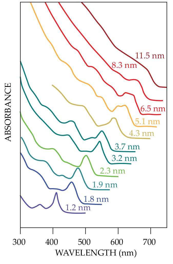
Figure
Figure 1.

Cadmium selenide nanocrystals absorb and emit differently colored light depending solely on the semiconductor’s size. Moungi Bawendi and his then graduate students Christopher Murray and David Norris developed a synthesis technique in 1993 to make defect-free semiconductor nanocrystals with narrow size distributions. (Adapted from ref.
Detectors and displays
Shortly before publishing the 1993 paper, Bawendi’s three graduate students—Murray, Nirmal, and Norris—went to their first conference to present the results. “And I still remember,” says Norris, “nobody was interested in our posters. All three of us were just completely depressed after that.”
Nirmal and Norris graduated from MIT in the mid 1990s and pursued other research, unsure if nanocrystals were a good topic to continue with in their careers. Only after a few years of the community tinkering with the new synthesis method with other materials did the possible applications become apparent.
Today some research groups are working on IR detectors based on quantum dots. Similar to how they can emit specific wavelengths of light in the visible range, quantum dots can be tuned for different IR wavelengths and then spread across a substrate. The layer could be incorporated into a highly sensitive camera. On a car, for example, such a detector could more clearly illuminate people and pets not visible from the road.
Quantum-dot-based detectors in the near-IR work, but the technology gets worse at the mid-IR and at longer wavelengths. “We’re using photon detectors, which can do high-speed observations, but they have to be cooled with liquid nitrogen, and they are super expensive, around $50 000 each,” says University of Chicago’s Philippe Guyot-Sionnest.
More basic research needs to be done before an IR detector based on quantum dots is a commercial possibility. But if the remaining challenges can be surmounted, Guyot-Sionnest says, “in principle, this would lead to very, very low cost infrared images that would slash the cost down by a factor of 1000.”
Now you don’t need to be a synthetic chemist to work with quantum dots. They’re for sale in various sizes at scientific supply retailers and are capable of emitting specific wavelengths to suit all sorts of requirements. And they’re already available in some consumer products too.
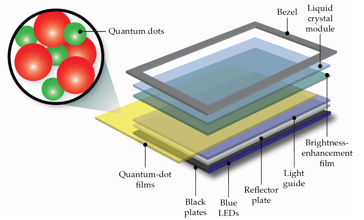
The ”Q” in Samsung’s QLED TVs, for example, stands for the monolayer of quantum dots that’s included in the screen, shown in figure
Figure 2.

Quantum dots are used in some new TVs and other displays. A blue LED backlight illuminates a thin film of quantum dots, which in their excited state emit brighter light than an LCD screen. Quantum-dot TVs also have larger color ranges, require less power, and can be incorporated into bigger and more-flexible displays. (Jyurek/Wikimedia Commons/CC BY-SA 3.0 .)
References
1. A. I. Ekimov, A. A. Onushchenko, Pis’ma Zh. Eksp. Teor. Fiz. 34, 363 (1981);
translated in A. I. Ekimov, A. A. Onushchenko, JETP Lett. 34, 345, (1982).2. R. Rossetti, S. Nakahara, L. E. Brus, J. Chem. Phys. 79, 1086 (1983). https://doi.org/10.1063/1.445834
3. A. L. Efros, L. E. Brus, ACS Nano 15, 6192 (2021). https://doi.org/10.1021/acsnano.1c01399
4. C. B. Murray, D. J. Norris, M. G. Bawendi, J. Am. Chem. Soc. 115, 8706 (1993). https://doi.org/10.1021/ja00072a025
5. M. A. Hines, P. Guyot-Sionnest, J. Phys. Chem. 100, 468 (1996). https://doi.org/10.1021/jp9530562
More about the authors
Alex Lopatka, alopatka@aip.org


