An Optical Probe Can Map Quantum Dot Wavefunctions
DOI: 10.1063/1.1634520

Improved fabrication methods that have allowed researchers to make smaller and smaller nanoscale structures have also fueled the need for new high-resolution tools capable of studying those structures. Semiconductor quantum dots (QDs), in which electrons are confined in all three dimensions, form an archetypical nanostructure. QDs can be imaged with scanning electron microscopy (SEM) and studied electrically if measurement circuitry is fabricated around the dots as the dots are being made. Optical studies of QDs are more challenging, because a dot’s typical size—from one to a few hundred nanometers—is well below the wavelength of light.
Still, optical techniques have revealed much about QDs. By sending in sufficiently energetic photons, one can excite an electron across the dot’s bandgap. The excited electron and resulting hole left in the valence band form a bound pair called an exciton; such pairs constitute the fundamental excitations of quantum dots. By monitoring the photoluminescence—that is, the light emitted when an exciton’s electron and hole recombine—one can measure the dot’s excitation spectrum, which reveals discrete energy states with detailed fine structure. In addition, polarized light can be used to modify the spin states of QDs. (See the article by Dan Gammon and Duncan Steel in Physics Today, October 2002, page 36 )
Now, using near-field optical spectroscopy, a team of researchers has gained new insight into QDs by successfully peering inside them. With their technique, capable of 30-nm resolution, they mapped the wavefunctions of quantum states in the dot for the first direct look at the dot’s fundamental excitations. 1 The collaboration consisted of Kazunari Matsuda and Toshiharu Saiki of the Kanagawa Academy of Science and Technology in Kawasaki, Japan, together with Shintaro Nomura, Masaru Mihara, and Yoshinobu Aoyagi of the Institute of Physical and Chemical Research (RIKEN) in Wako, Japan, Selvakumar Nair of the University of Toronto, and Toshihide Takagahara of the Kyoto Institute of Technology.
Beating the diffraction limit
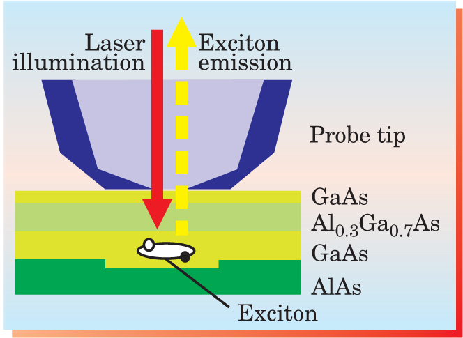
In most situations, diffraction restricts the spatial resolution of an optics system to half the wavelength of the light being used. But the diffraction limit can be circumvented by working in the near field: keeping the size of optical elements and the distance to the sample shorter than a wavelength. Near-field scanning optical microscopy (NSOM)—and its cousin, near-field scanning optical spectroscopy—take advantage of the potential gains in resolution by sweeping the tip of an optical fiber, narrowed to sub-wavelength diameter, very closely over the sample being studied (see figure 1). In the near field, the resolution is limited by the geometry of the optics system: the diameter of the fiber’s tip and the separation distance between the tip and the sample.

Figure 1. Near-field scanning optical microscopy of quantum dots relies on getting a narrow-aperture fiber-optic probe very close to the quantum dot formed in a semiconductor heterostructure. With this technique, the wavefunction of an electron-hole pair (an exciton) in the dot has been mapped.
(Adapted from ref. 1.)
Harold Hess, Eric Betzig, and colleagues at Bell Labs reported the first low-temperature NSOM of QDs nearly 10 years ago. 2 With a resolution of about 100 nm, they were able to identify QDs that occurred spontaneously in a two-dimensional quantum well as the localized sources of individual photoluminescence emission lines. Although that work demonstrated the potential of NSOM in nanotechnology, “the performance of NSOM has not drastically progressed in terms of sensitivity and spatial resolution,” notes Matsuda.
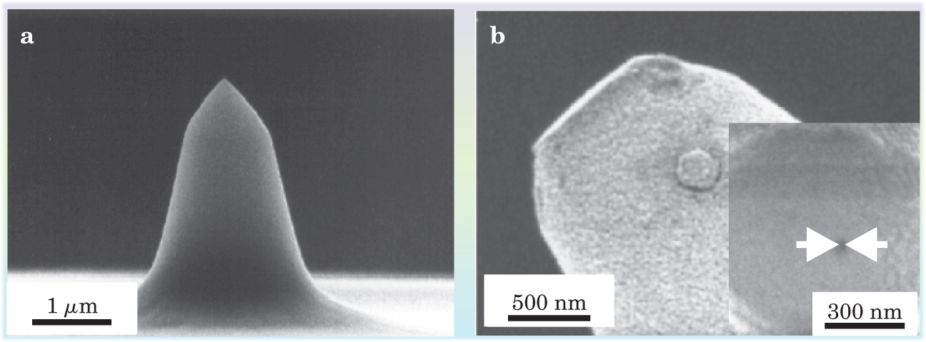
The key improvement in resolution achieved by Saiki and colleagues is the engineering of their NSOM tip. Figure 2 shows the shape of the doubly tapered tip they fashioned in a two-step chemical etching process. After coating the tip with gold, the researchers opened a hole by controllably pounding the tip against the sample surface as they monitored the emitted light intensity. (A similar pounding technique was used to form the aperture in the first demonstration of near-field optical microscopy 3 ) The result, as estimated from SEM images, was an aperture diameter of only 20 nm.

Figure 2. The fiber-optic tip is a critical part of a near-field scanning optical microscopy experiment, (a) A side view of the initial dual-taper shape of the tip used by Toshiharu Saiki and colleagues to map exciton wavefunctions. (b) A side view of the blunted tip after it has been pounded against the sample surface to open a hole in the tip. A top view (inset) reveals the 20-nm aperture.
(Courtesy of K. Matsuda.)
Using a different technique that, like a lightning rod, concentrates electric fields with a bare ultrasharp metal tip, Lukas Novotny (University of Rochester) and colleagues have obtained 25-nm-resolution images of carbon nanotubes with near-field optical Raman microscopy 4
Mapping a dot
Matsuda and Saiki used their NSOM probe to study spontaneously formed QDs in semiconductor heterostructures. To make the dots, collaborators Nomura and Mihara used molecular beam epitaxy to sandwich a 5-nm layer of gallium arsenide between layers of aluminum arsenide and aluminum gallium arsenide. Two-minute interruptions of the deposition at both interfaces promoted the formation of monolayer-high steps. Those variations in the thickness of the GaAs layer produced variations in the potential energy landscape sufficient to localize electrons in a disk-shaped box in the GaAs layer about 230 nm in diameter and 5 nm tall. Separating the NSOM probe tip from the dot were the 15-nm AlGaAs layer and a 5-nm GaAs capping layer (see figure 1). The 20-nm distance was sufficiently close to avoid a major reduction in the NSOM resolution: The aperture and tip-sample dimensions combined to give a resolution of 30 nm, or about 1/25 of the wavelength emitted by excitons.
The researchers placed their QD sample and their NSOM tip, mounted on a piezoelectric scanner, inside a cryostat cooled to a temperature of 9 K. The tip served a dual purpose. Light from a helium-neon laser coupled to the optical fiber emerged from the tip to create excitons in the sample. The tip also collected the photoluminescence emitted from recombining excitons; the collected signal was separated by room-temperature optics and sent to a sensitive spectrometer. Because the charges excited by the incoming radiation were quite mobile and rapidly diffused away from the NSOM tip, the imaging resolution came solely from the tip’s narrow light-collection window.
An exciton’s electron and hole attract each other, just like the electron and proton in a hydrogen atom. The hole is much lighter than a proton; the smaller reduced mass and the larger dielectric constant in the QD make an exciton’s Bohr radius (its characteristic size) about 10 nm. The exciton thus behaves like a tightly bound composite hydrogen-like particle confined within a much larger box. Because an exciton’s electron and hole can recombine only when they overlap, the spatial distribution of the photoluminescence signal depends only on the composite center-of-mass component of the wavefunction.
For sufficiently strong laser excitation, the photoluminescence signal that reaches the detector has two sharp peaks in its spectrum. The stronger, higher-energy peak is the signal emitted by a single exciton when its constituent electron and hole recombine. The smaller peak at slightly lower energy is the signal emitted by a two-exciton state (a so-called biexciton) when one of the excitons recombines, leaving a single exciton in the dot. Because of the interactions between the excitons, the energy of the biexciton state is slightly less than twice that of the exciton state.
The energy difference allowed the researchers, by scanning the NSOM tip across the sample, to map separately the spatial dependence of the exciton and biexciton photoluminescence. Figure 3 shows the exciton and biexciton photoluminescence intensities detected in a QD that’s elongated along the [|10] crystal direction. Both show a similar shape, but the biexciton signal is more spatially confined than the exciton signal.

Figure 3. Exciton and biexciton maps. The energies of photons given off by excitons and biexcitons differ slightly. That difference allows separate mapping of the spatial extent of the photo-luminescence from (a) excitons and (b) biexcitons. Both states show elongation along one crystal direction, but the biexciton emission is more confined.
(Adapted from ref. 1.)
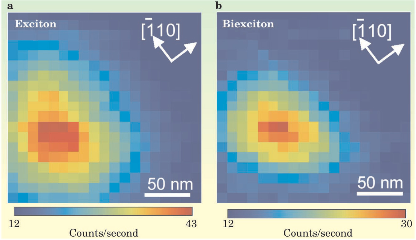
With the help of theoretical calculations by Nair and Takagahara, the collaboration showed that the different photoluminescence distributions reflect the different wavefunction distributions of the exciton and biexciton. For the exciton, the photoluminescence distribution is, to a first approximation, proportional to the square of the exciton’s center-of-mass wavefunction; figure 3a is thus a map of the center-of-mass component of the exciton wavefunction. For the biexciton, the calculations are more involved but yield a clear result: The tighter spatial confinement of the biexciton emission is a consequence of the attraction and correlation between the two excitons. Calculations of the emission patterns expected from excitons and biexcitons in disk-shaped QDs of the size the team studied bear out that conclusion: The theoretical ratio of widths, 0.76, is in good agreement with the experimental result, 0.72 ± 0.08.
If QDs are ever harnessed for processing quantum information, notes Garnett Bryant (NIST, Gaithersburg, Maryland), getting detailed information about the wavefunction will be invaluable. But for now, the information will likely be of more fundamental interest. Whereas the physical size of QDs can be measured with other techniques like SEM, the actual confinement potential can be very different from the physical geometry due to strains, surface charges, and other factors; now with NSOM one can begin to see those effects directly. The attainable resolution is currently smaller than the largest QDs and is approaching the size of excitons. The ultimate insight into exciton states will come if the optical resolution can approach 1 nm, but that, says Bryant, “will be awfully hard to achieve.”
References
1. K. Matsuda, T. Saiki, S. Nomura, M. Mihara, Y. Aoyagi, S. Nair, T. Takagahara, Phys. Rev. Lett, (in press).
2. H. F. Hess et al., Science 264, 1740 (1994) https://doi.org/10.1126/science.264.5166.1740 .
3. D. W. Pohl, W. Denk, M. Lanz, Appl. Phys. Lett. 44, 651 (1984) https://doi.org/10.1063/1.94865 .
4. A. Hartschuh et al., Phys. Rev. Lett. 90, 095503 (2003) https://doi.org/10.1103/PhysRevLett.90.095503 .
More about the authors
Richard J. Fitzgerald, rfitzger@aip.org


