The quantum spin Hall effect and topological insulators
DOI: 10.1063/1.3293411
In the quantum world, atoms and their electrons can form many different states of matter, such as crystalline solids, magnets, and superconductors. Those different states can be classified by the symmetries they spontaneously break—translational, rotational, and gauge symmetries, respectively, for the examples above. Before 1980 all states of matter in condensed-matter systems could be classified by the principle of broken symmetry. The quantum Hall (QH) state, discovered in 1980, 1 provided the first example of a quantum state that has no spontaneously broken symmetry. Its behavior depends only on its topology and not on its specific geometry; it was topologically distinct from all previously known states of matter.
Recently, a new class of topological states has emerged, called quantum spin Hall (QSH) states or topological insulators (see Physics Today, January 2008, page 19 ). Topologically distinct from all other known states of matter, including QH states, QSH states have been theoretically predicted and experimentally observed in mercury telluride quantum wells, 2,3 in bismuth antimony alloys, 4,5 and in Bi2Se3 and Bi2Te3 bulk crystals. 6–8 QSH systems are insulating in the bulk—they have an energy gap separating the valence and conduction bands—but on the boundary they have gapless edge or surface states that are topologically protected and immune to impurities or geometric perturbations. 9–12 Inside such a topological insulator, Maxwell’s laws of electromagnetism are dramatically altered by an additional topological term with a precisely quantized coefficient, 12 which gives rise to remarkable physical effects. Whereas the QSH state shares many similarities with the QH state, it differs in important ways. In particular, QH states require an external magnetic field, which breaks time-reversal (TR) symmetry; QSH states, in contrast, are TR invariant and do not require an applied field.
From quantum Hall to quantum spin Hall
In a one-dimensional world, there are two basic motions: forward and backward. Random scattering can cause them to mix, which leads to resistance. Just as we have learned from basic traffic control, it would be much better if we could spatially separate the counterflow directions into two separate lanes, so that random collisions could be easily avoided. That simple traffic control mechanism turns out to be the essence of the QH effect. 1
The QH effect occurs when a strong magnetic field is applied to a 2D gas of electrons in a semiconductor. At low temperature and high magnetic field, electrons travel only along the edge of the semiconductor, and the two counterflows of electrons are spatially separated into different “lanes” located at the sample’s top and bottom edges. Compared with a 1D system with electrons propagating in both directions, the top edge of a QH bar contains only half the degrees of freedom. That unique spatial separation is illustrated in figure 1a by the symbolic equation “2 = 1 [forward mover] + 1 [backward mover]” and is the key reason why the QH effect is topologically robust. When an edge-state electron encounters an impurity, it simply takes a detour and still keeps going in the same direction (figure

Figure 1. Spatial separation is at the heart of both the quantum Hall (QH) and the quantum spin Hall (QSH) effects. (a) A spinless one-dimensional system has both a forward and a backward mover. Those two basic degrees of freedom are spatially separated in a QH bar, as illustrated by the symbolic equation “2 = 1 + 1.” The upper edge contains only a forward mover and the lower edge has only a backward mover. The states are robust: They will go around an impurity without scattering. (b) A spinful 1D system has four basic channels, which are spatially separated in a QSH bar: The upper edge contains a forward mover with up spin and a backward mover with down spin, and conversely for the lower edge. That separation is illustrated by the symbolic equation “4 = 2 + 2.”
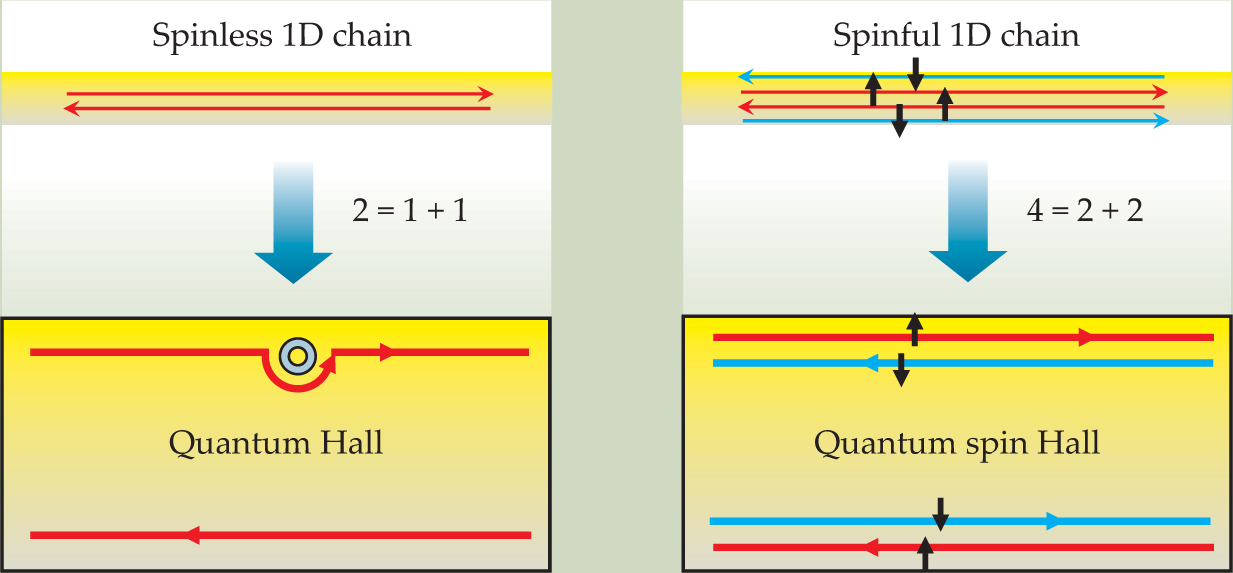
Can we get rid of the magnetic field and still separate the traffic lanes for the electrons? In a real 1D system, forward-and backward-moving channels for both spin-up and spin-down electrons give rise to four channels, as shown in figure
Although a QSH edge consists of both backward and forward movers, backscattering by nonmagnetic impurities is forbidden. To understand that effect, we start with an analogy from daily life. Most eyeglasses and camera lenses have a so-called antireflection coating. As shown in figure 2a, reflected light from the top and the bottom surfaces interfere with each other destructively, leading to zero net reflection and thus perfect transmission. However, such an effect is not robust, as it depends on the matching between the optical wavelength and the thickness of the coating.

Figure 2. (a) On a lens with antireflection coating, light waves reflected by the top (blue line) and the bottom (red line) surfaces interfere destructively, which leads to suppressed reflection. (b) A quantum spin Hall edge state can be scattered in two directions by a nonmagnetic impurity. Going clockwise along the blue curve, the spin rotates by π; counterclockwise along the red curve, by −π. A quantum mechanical phase factor of −1 associated with that difference of 2π leads to destructive interference of the two paths—the backscattering of electrons is suppressed in a way similar to that of photons off the antireflection coating.
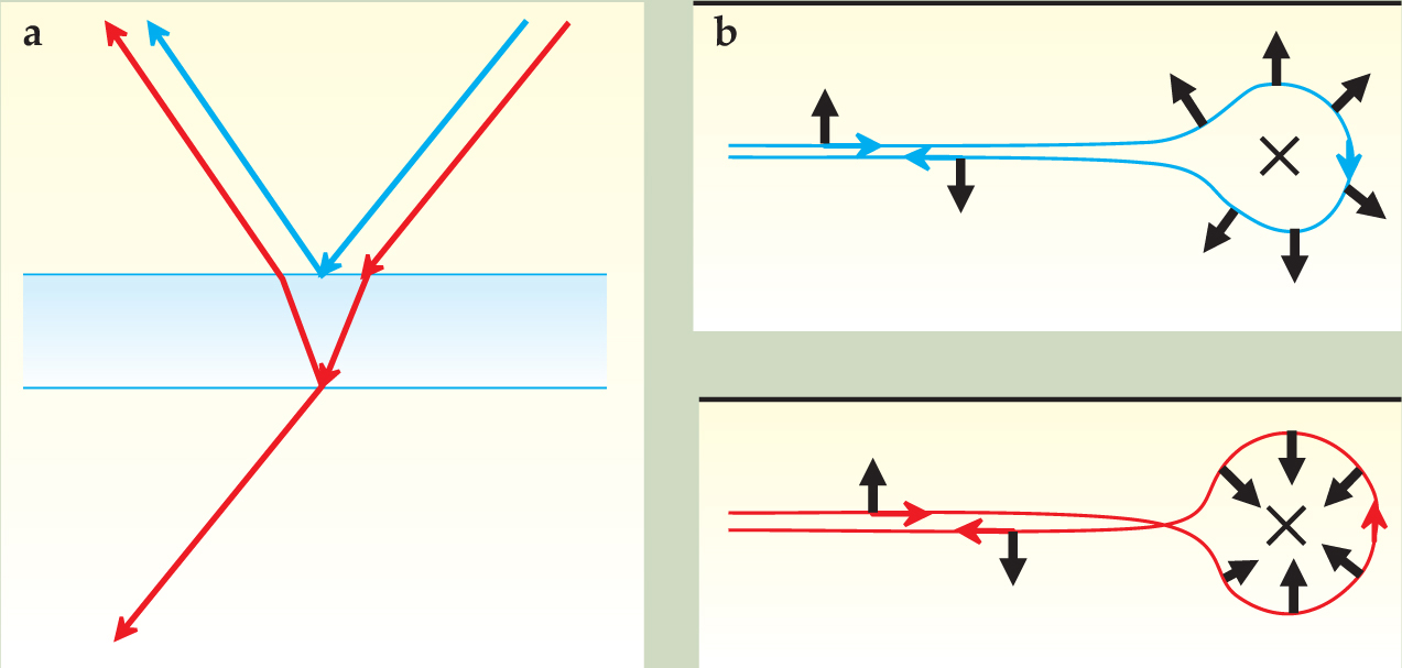
Just like the reflection of a photon by a surface, an electron can be reflected by an impurity, and different reflection paths also interfere with each other. As shown in figure
The physical picture above applies only to the case of single pairs of QSH edge states. If there are two forward movers and two backward movers in the system—as, for example, the unseparated 1D system shown in figure
Two-dimensional topological insulators
Looking at figure
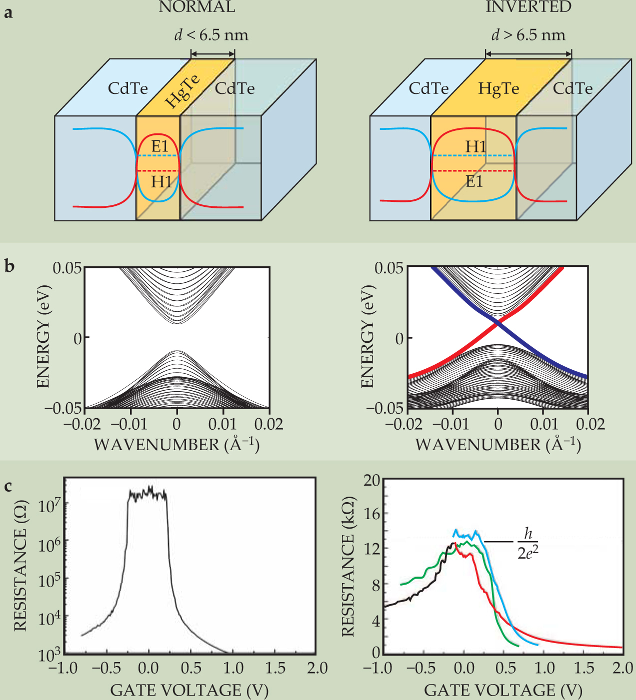
In most common semiconductors, the conduction band is formed from electrons in s orbitals and the valence band is formed from electrons in p orbitals. In certain heavy elements such as Hg and Te, however, the spin–orbit coupling is so large that the p-orbital band is pushed above the s-orbital band—that is, the bands are inverted. Mercury telluride quantum wells can be prepared by sandwiching the material between cadmium telluride, which has a similar lattice constant but much weaker spin–orbit coupling. Therefore, increasing the thickness d of the HgTe layer increases the strength of the spin–orbit coupling for the entire quantum well. For a thin quantum well, as shown in the left column of figure 3a, the CdTe has the dominant effect and the bands have a normal ordering: The s-like conduction subband E1 is located above the p-like valence subband H1. In a thick quantum well, as shown in the right column, the opposite ordering occurs due to increased thickness d of the HgTe layer. The critical thickness d c for band inversion is predicted to be around 6.5 nm.

Figure 3. Mercury telluride quantum wells are two-dimensional topological insulators. (a) The behavior of a mercury telluride–cadmium telluride quantum well depends on the thickness d of the HgTe layer. Here the blue curve shows the potential-energy well experienced by electrons in the conduction band; the red curve is the barrier for holes in the valence band. Electrons and holes are trapped laterally by those potentials but are free in the other two dimensions. For quantum wells thinner than a critical thickness d c ≃ 6.5 nm, the energy of the lowest-energy conduction subband, labeled E1, is higher than that of the highest-energy valence band, labeled H1. But for d > d c, those electron and hole bands are inverted. (b) The energy spectra of the quantum wells. The thin quantum well has an insulating energy gap, but inside the gap in the thick quantum well are edge states, shown by red and blue lines. (c) Experimentally measured resistance of thin and thick quantum wells, plotted against the voltage applied to a gate electrode to change the chemical potential. The thin quantum well has a nearly infinite resistance within the gap, whereas the thick quantum well has a quantized resistance plateau at R = h/2e 2, due to the perfectly conducting edge states. Moreover, the resistance plateau is the same for samples with different widths, from 0.5 µm (red) to 1.0 µm (blue), proof that only the edges are conducting.
The QSH state in HgTe can be described by a simple model for the E1 and H1 subbands
2
(see the
Less than one year after the theoretical prediction, a team at the University of Würzburg led by Laurens Molenkamp observed the QSH effect in HgTe quantum wells grown by molecular-beam epitaxy.
3
The edge states provide a direct way to experimentally distinguish the QSH insulator from the trivial insulator. The two edge states of the QSH insulator act as two conducting 1D channels, which each contribute one quantum of conductance, e 2/h. That perfect transmission is possible because of the principle of antireflection explained earlier. In contrast, a trivial insulator phase is “really” insulating, with vanishing conductance. Such a sharp conductance difference between thin and thick quantum wells was observed experimentally, as shown in figure
From two to three dimensions
From figure

Figure 4. In three-dimensional topological insulators, the linearly dispersing edge states of figure
Liang Fu and Kane predicted
4
that the alloy Bi1−x Sb x would be a 3D topological insulator in a special range of x, and with angle-resolved photoemission spectroscopy (ARPES) Zahid Hasan and coworkers at Princeton University observed the topological surface states in that system.
5
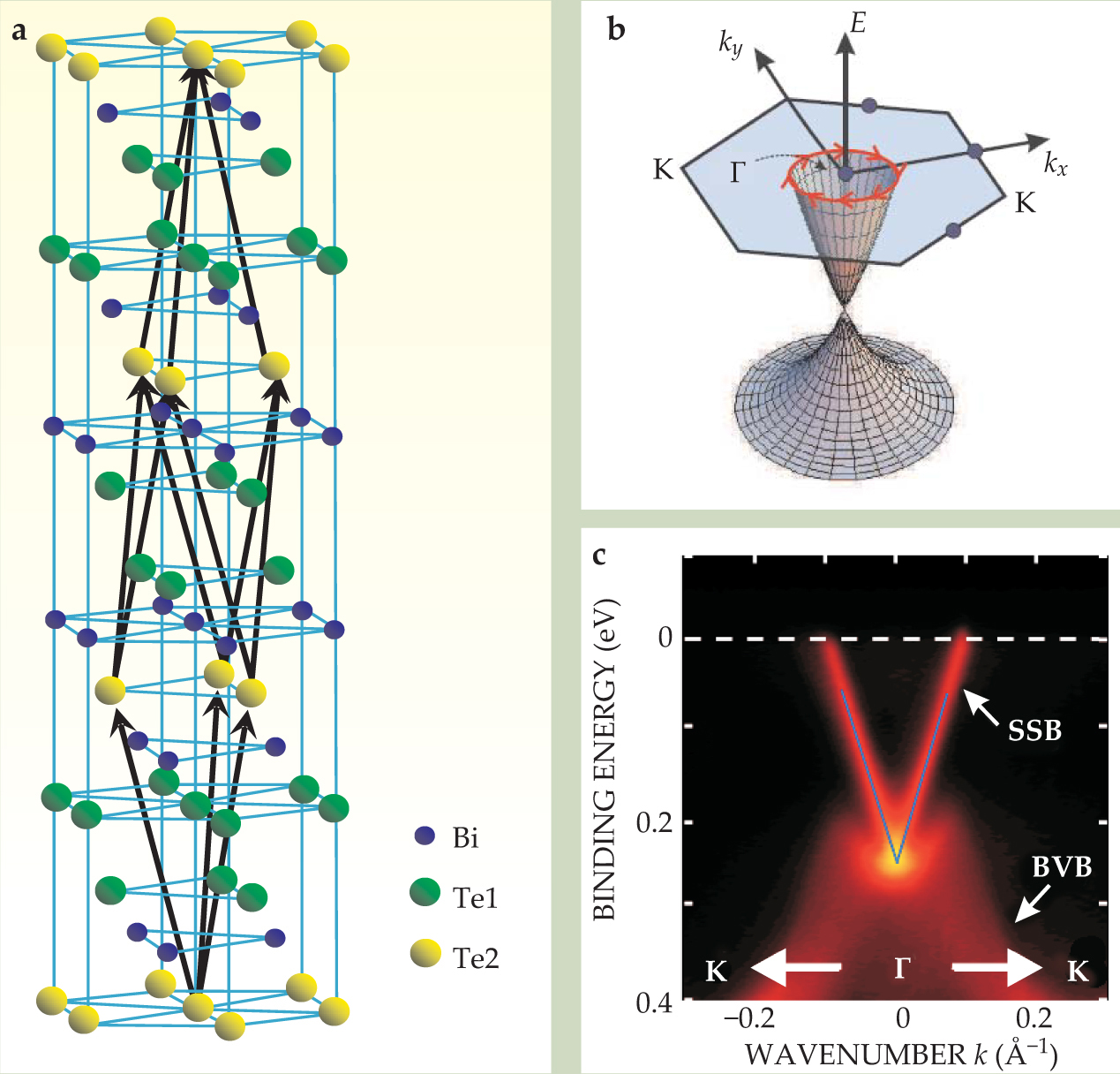
However, the surface states and the underlying mechanism turn out to be extremely complex. In collaboration with Zhong Fang’s group at the Chinese Academy of Sciences, the two of us predicted that Bi2Te3, Bi2Se3, and Sb2Te3, all with the layered structure in figure
As in HgTe, the nontrivial topology of the Bi2Te3 family is due to band inversion between two orbitals with opposite parity, driven by the strong spin–orbit coupling of Bi and Te. Due to such similarity, that family of 3D topological insulators can be described by a 3D version of the HgTe model (see the
Known to be excellent thermoelectric materials, Bi2Te3 and Bi2Se3 have been investigated independently, particularly at Princeton, where Hasan’s group observed in ARPES experiments the single Dirac-cone surface state of Bi2Se3 samples prepared by Robert Cava and coworkers.
7
Furthermore, the group’s spin-resolved measurements showed that the electron spin indeed lies in the plane of the surface and is always perpendicular to the momentum, in agreement with theory. However, the experiments also observed bulk carriers coexisting with the topological surface states. A pure topological-insulator phase without bulk carriers was first observed in Bi2Te3 by Yulin Chen and Zhi-xun Shen’s group at Stanford in ARPES experiments on material prepared by Ian Fisher and colleagues.
8
As shown in figure
Models of topological insulators
The essence of the quantum spin Hall effect in real materials can be captured in explicit models that are particularly simple to solve. The two-dimensional topological insulator mercury telluride can be described by an effective Hamiltonian that is essentially a Taylor expansion in the wave vector k of the interactions between the lowest conduction band and the highest valence band:
2
The 3D topological insulator in the Bi2Te3 family can be described by a similar model:
6
Topological classification of insulators
Mathematicians group geometric objects into broad topological classes. Objects with different shapes, such as a donut and a coffee cup, can be smoothly deformed into each other and can therefore be grouped into the same topological class. Mathematicians also developed the concept of a topological invariant that uniquely defines the topological class. Topological materials in general, and topological insulators in particular, can be defined by physically measurable topological invariants in topological field theories.
We can first divide insulators into two broad classes, according to the presence or absence of TR symmetry. The QH state is a topological insulator state that breaks TR symmetry. David Thouless and coworkers showed that the physically measured integer QH conductance is given by a topological invariant called the first Chern number (see the article by Joseph Avron, Daniel Osadchy, and Ruedi Seiler, Physics Today, August 2003, page 38 ). For a generally interacting system, the topological properties of the QH state can be described by an effective topological field theory based on the Chern–Simons theory. 14 Although Duncan Haldane constructed a model of the QH effect without the external magnetic field, that state still breaks TR symmetry.
For a long time it was widely believed that both TR symmetry breaking and two-dimensionality are necessary for an insulator to be topological, but in 2001 the first model of a TR-invariant topological insulator was introduced. 15 That model was originally defined in 4D, but TR-invariant topological insulators in 3D and 2D can be obtained through a simple dimension-reduction procedure. 12 Shuichi Murakami, Naoto Nagaosa, and Zhang, and in parallel MacDonald and colleagues at the University of Texas in Austin, developed the theory of the intrinsic spin Hall effect in doped semiconductors and identified spin–orbit coupling as the crucial ingredient; later, Murakami, Nagaosa, and Zhang extended the theory to TR-invariant insulators. Kane and Mele first introduced the topological band theory of TR-invariant QSH insulators in 2D and showed that they fall into two distinct topological classes, generally referred to as the Z 2 classification. 9 That beautiful topological band theory was soon generalized to three dimensions. 11 The two of us and our colleagues have developed a unifying topological field theory that defines the general concept of a topological insulator in terms of a physically measurable topological field theory. 12
We now have two precise definitions of TR-invariant topological insulators, one in terms of noninteracting topological band theory 11 and one in terms of topological field theory. 12 If we approximate an insulator with noninteracting electrons filling a certain number of bands, the topological band theory can evaluate an explicit topological invariant that can give only binary values of 0 or 1: a Z 2 classification that defines trivial and nontrivial insulators. For materials with inversion symmetry, a powerful algorithm developed by Fu and Kane 4 can be easily integrated into electronic structure calculations to numerically evaluate the topological band invariant. However, since all insulators in nature are necessarily interacting, it is important to have a general definition of topological insulators that is valid for interacting systems and is experimentally measurable. Both problems were solved with the topological field theory, 12 which can be generally defined for all insulators, with or without interactions. In the noninteracting case, both definitions agree. Surprisingly, the topological field theory can be explained in terms of elementary concepts in undergraduate-level electromagnetism.
Inside an insulator, the electric field E and the magnetic field B are both well defined. In a Lagrangian-based field theory, the insulator’s electromagnetic response can be described by the effective action
There is, however, another possible term in the action of the electromagnetic field:
Since the E field is invariant under TR, whereas the B field changes sign, S θ naively breaks TR symmetry. For a periodic system, however, there are two values of θ, namely θ = 0 or θ = π, that preserve the TR symmetry. 12 One can easily understand that conclusion by an analogy. If we have a 1D ring with a magnetic flux inside, a general value of the flux Φ would break the TR symmetry. However, for two special values of the flux, Φ = 0 or Φ = hc/2e, an electron’s wavefunction changes its phase by 0 or π when the electron circles the ring either clockwise or counterclockwise, and TR symmetry is maintained.
If we integrate out all the microscopic fermionic degrees of freedom to obtain the effective action S θ , all nonmagnetic insulators in the universe would fall into two distinct topological classes, described by effective topological field theories with θ = 0 or with θ = π. Unlike ϵ and µ, the physically measurable θ parameter is universally quantized, with the two possible values defining the topologically trivial and nontrivial insulators, respectively—the Z 2 classification again.
Such classification is valid for a periodic system. For a real solid with a finite boundary, a topological insulator is insulating only in the bulk; it has an odd number of gapless Dirac cones on the surface that describe conducting surface states. If we uniformly cover the surface with a thin ferromagnetic film, an insulating gap also opens up on the boundary; the TR symmetry is preserved in the bulk but broken on the surface. The last identity of the equation above for S θ shows that the bulk topological term is in fact a total derivative, expressible as a surface term, given by the expression in parenthesis. That surface term is the same Chern–Simons term that describes the topological field theory of the QH state. In the QH field theory, the term’s coefficient specifies the value of the Hall conductance.
14
Here the coefficient of θ = π translates into a Hall conductance of
Outlook
The field of topological insulators is growing rapidly, and many remarkable experiments have been carried out. In nonlocal transport measurements in a series of HgTe devices, the Würzburg group confirmed that transport current is carried by the QSH edge states. The topological insulators Bi2Te3 and Bi2Se3 fabricated in nanoribbon form at Stanford and by molecular-beam epitaxy at Tsinghua University. Scanning tunneling microscopy experiments have been carried out at Princeton, Stanford, and Tsinghua universities to probe the topological surface states. Preliminary transport measurements indicate dominant contributions from surface states.
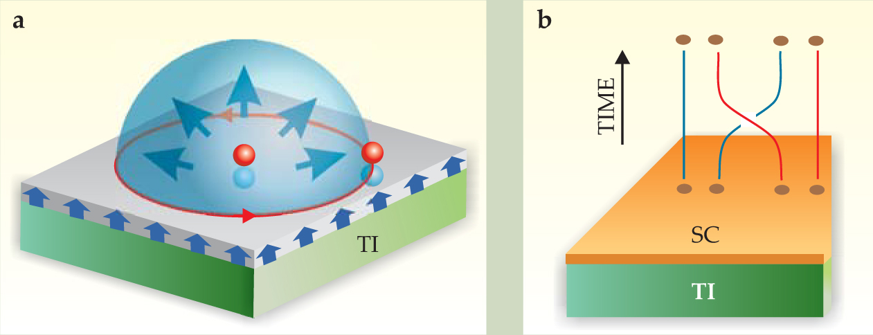
Solving Maxwell’s equations with the topological term included leads to predictions of novel physical properties characterized by exotic excitations. The 2D QSH insulator is predicted to have fractional charge at the edge and spin–charge separation in the bulk. In introductory physics classes we learned that a point charge above a metal or an insulator can be viewed as inducing an image charge below the surface. A point charge above the surface of a 3D topological insulator is predicted to induce not only an image electric charge but also an image magnetic monopole below the surface, 12 as shown in figure 5a. Such a composite object of electric and magnetic charges, called a dyon, would obey neither Bose nor Fermi statistics but would behave like a so-called anyon with any possible statistics. Dislocations inside a 3D topological insulator contain electronic states that behave similarly to QSH edge states.

Figure 5. Novel behavior is predicted for topological insulators. (a) When a topological insulator (TI, green) is coated by a thin ferromagnetic layer (gray), each electron (red sphere) in the vicinity of the surface induces an image monopole (blue sphere) right beneath it.
Axions are weakly interacting particles postulated to solve some puzzles in the standard model of particle physics
16
(see the article by Karl van Bibber and Leslie Rosenberg, Physics Today, August 2006, page 30 ). Those elusive particles are also predicted to exist inside topological magnetic insulators, systems for which the θ parameter above becomes dependent on position and time. Majorana fermions are distinct from the familiar Dirac fermions: They are their own antiparticles. There is still no conclusive evidence for Majorana fermions in nature. But when a superconductor is close to the surface of a topological insulator, Majorana fermions are predicted to occur inside vortices (see figure
Besides teaching us about the quantum world, the exotic particles in topological insulators could find novel uses. For example, image monopoles could be used to write magnetic memory by purely electric means, and the Majorana fermions could be used for topological quantum computing. 18
Albert Einstein insisted that all fundamental laws of physics should be expressed in terms of geometry, and he exemplified that ancient Greek ideal by formulating the theory of gravity in terms of the geometrical curvature of space and time. Physicists are now pursuing Einstein’s dream one step further, exploring the fundamental laws expressed in terms of topological field theory. The standard model of elementary particles contains a topological term that is identical to the S θ term that defines topological insulators. Even if only a small number of the predicted exotic particles are observed in topological insulators, our fundamental understanding of nature would be greatly enhanced. Such tabletop experiments could become a window into the standard model 16 and help reveal the alluring beauty and mysteries of our universe.
References
1. K. v. Klitzing, G. Dorda, M. Pepper, Phys. Rev. Lett. 45, 494 (1980). https://doi.org/10.1103/PhysRevLett.45.494
2. B. A. Bernevig, T. L. Hughes, S.-C. Zhang, Science 314, 1757 (2006). https://doi.org/10.1126/science.1133734
3. M. König et al., Science 318, 766 (2007). https://doi.org/10.1126/science.1148047
4. L. Fu, C. L. Kane, Phys. Rev. B 76, 045302 (2007). https://doi.org/10.1103/physrevb.76.045302
5. D. Hsieh et al., Nature 452, 970 (2008). https://doi.org/10.1038/nature06843
6. H. Zhang et al., Nat. Phys. 5, 438 (2009). https://doi.org/10.1038/nphys1674
7. Y. Xia et al., Nat. Phys. 5, 398 (2009); https://doi.org/10.1038/nphys2256
D. Hsieh et al., Science 323, 919 (2009). https://doi.org/10.1126/science.11677338. Y. L. Chen et al., Science 325, 178 (2009). https://doi.org/10.1126/science.1173034
9. C. L. Kane, E. J. Mele, Phys. Rev. Lett. 95, 226801 (2005); https://doi.org/10.1103/PhysRevLett.95.226801
C. L. Kane, E. J. Mele, Phys. Rev. Lett. 95, 146802 (2005). https://doi.org/10.1103/PhysRevLett.95.14680210. B. A. Bernevig, S.-C. Zhang, Phys. Rev. Lett. 96, 106802 (2006). https://doi.org/10.1103/PhysRevLett.96.106802
11. J. E. Moore, L. Balents, Phys. Rev. B 75, 121306 (2007); https://doi.org/10.1103/physrevb.75.121306
L. Fu, C. L. Kane, E. J. Mele, Phys. Rev. Lett. 98, 106803 (2007); https://doi.org/10.1103/PhysRevLett.98.106803
R. Roy, Phys. Rev. B 79, 195322 (2009). https://doi.org/10.1103/physrevb.79.19532212. X.-L. Qi, T. L. Hughes, S.-C. Zhang, Phys. Rev. B 78, 195424 (2008); https://doi.org/10.1103/physrevb.78.195424
X.-L. Qi et al., Science 323, 1184 (2009). https://doi.org/10.1126/science.116774713. C. Wu, B. A. Bernevig, S.-C. Zhang, Phys. Rev. Lett. 96, 106401 (2006); https://doi.org/10.1103/PhysRevLett.96.106401
C. Xu, J. E. Moore, Phys. Rev. B 73, 045322 (2006). https://doi.org/10.1103/physrevb.73.04532214. S.-C. Zhang, Int. J. Mod. Phys. B 6, 25 (1992). https://doi.org/10.1142/S0217979292000037
15. S.-C. Zhang, J. Hu, Science 294, 823 (2001). https://doi.org/10.1126/science.294.5543.823
16. F. Wilczek, Nature 458, 129 (2009); https://doi.org/10.1038/458129e
F. Wilczek, Nat. Phys. 5, 614 (2009). https://doi.org/10.1038/nphys138017. L. Fu, C. L. Kane, Phys. Rev. Lett. 100, 096407 (2008). https://doi.org/10.1103/PhysRevLett.100.096407
18. C. Nayak et al., Rev. Mod. Phys. 80, 1083 (2008). https://doi.org/10.1103/RevModPhys.80.1083
More about the authors
Xiao-Liang Qi is a research associate at the Stanford Institute for Materials and Energy Science and Shou-Cheng Zhang is a professor of physics at Stanford University in Stanford, California.
Xiao-Liang Qi, 1 Stanford Institute for Materials and Energy Science, Stanford University, Stanford, California, US .
Shou-Cheng Zhang, 2 Stanford University, Stanford, California, US .


