Imaging Electron Flow
DOI: 10.1063/1.1650228
Semiconductor heterostructures have revolutionized solid-state physics and its applications. Most of us use the fruits of this revolution every day in CD and DVD recorders and players, cellular telephones, laser-based telecommunications, satellite television, and much more. The technology, based on atomic layer-by-layer growth using molecular beam epitaxy (MBE), is sophisticated, remarkable, and marketable.
One class of semiconductor heterostructures, the two-dimensional electron gas (2DEG), has been a focal point for theorists and experimentalists and a wellspring of new physics. A 2DEG can be produced at low temperatures at an interface of two distinct layers (a so-called heterojunction) doped nearby with atoms that donate electrons. The electrons at such a junction are confined to the lowest quantum state in the direction normal to the interface; by charging gate electrodes on the top surface of the heterostructure some distance away to repel them, the electrons can be further confined in the other directions to make dots, wires, resonators, and other shapes. That technology has led to celebrated discoveries including the integer and fractional quantum Hall effect (QHE), 1 the Coulomb blockade and single-electron transistors, and conductance quantization in quantum point contacts (QPCs). 2 The potential for exploiting these and many other quantum effects is spawning new fields of single electronics 3 and spintronics 4 —new approaches to logic that use single electron charges and spins to represent bits of data—and the new area of quantum information processing, based on the coherent interaction of quantum mechanical qubits. 5
Despite all the beautiful experiments already performed on 2DEGs and all that is riding on the new science and phenomena made possible by them, researchers have been blind until recently as to how electrons actually move through them. Most of the knowledge of electron flow in 2DEGs is indirect, based on electron-transport measurements of macroscopically averaged quantities. To be sure, many of the statistical properties are known, such as the electron mean free path. But macroscopically averaged parameters do not reveal the details of the fascinating behavior to be found on the nanoscale. For that, imaging is needed.
Imaging a system is essential to understanding its fundamental properties and developing new electronic and magnetic devices. Imagine the difficulty of designing and fabricating an integrated circuit from a silicon crystal without the use of an optical or electron microscope. As device sizes continue to decrease, quantum behavior becomes important and offers new research and application opportunities. To understand the fundamental behavior of electrons in this quantum regime and to make functioning devices based on this behavior, one must develop ways to visualize the flow of electron charges and spins through semiconductors. The invention of the scanning tunneling microscope (STM) allowed researchers to directly view the pattern of atoms on a material’s surface. Additional methods are needed to image the flow of electrons beneath the surface.
Obtaining images of 2DEGs inside semiconductors is no easy matter, because the electrons are buried beneath the surface and because the samples must be cooled to low temperatures to show quantum behavior. Nonetheless, a number of groups have recently developed liquid-helium–cooled scanning probe microscopes (SPM) for this purpose.
Making a two-dimensional electron gas
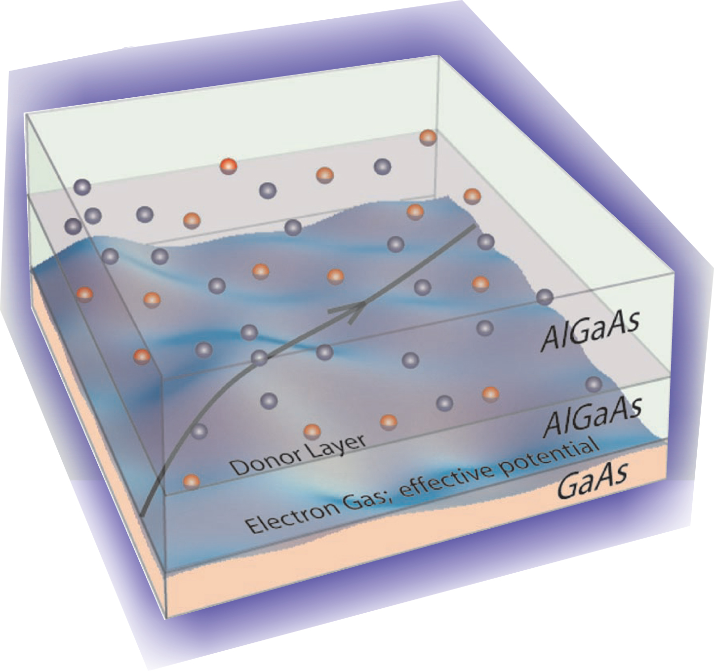
Figure 1 illustrates how a 2DEG can be created inside a gallium arsenide–aluminum gallium arsenide heterostructure. During growth by MBE, atomic layers are added to the heterostructure at a rate of about one layer per second. Conduction-band profiles can be engineered during growth by changing the Al fraction. Switching abruptly from GaAs to AlGaAs creates a very clean, sharp barrier that keeps electrons inside the GaAs layer. Silicon atoms in the AlGaAs layer act as donors: The electrons ionized from the Si fall over the barrier and are trapped at the GaAs–AlGaAs interface, where they can move freely for long distances. At low temperatures, movement in the z-direction (normal to the interface) is frozen out, but the electrons, trapped in a 2D “flatland” sheet, are free to move and interact in the x- and y-directions.

Figure 1. A two-dimensional electron gas formed at the interface between gallium arsenide and aluminum gallium arsenide in a semiconductor heterostructure. The AlGaAs layer (green) contains a layer (purple) of silicon donor atoms (dark blue). Electrons from the donor layer fall into the GaAs layer (pink) to form a 2DEG (blue) at the interface. The ionized Si donors (red) create a potential landscape for the electron gas; the resulting small-angle scattering smoothly bends electron trajectories, as shown.
Two-dimensional electron gases possess a unique combination of parameters that together make an ideal laboratory in which to explore the fascinating and often surprising behavior of such systems. The electron’s de Broglie wavelength at the Fermi energy is unusually long, typically 20–100 nm, and it can be an appreciable fraction of the size of a typical device. (Electron wavelengths in metals, by comparison, are typically well under 1 nm.) The Fermi wavelength can be tuned by changing the electron density with a planar gate electrode located beneath the 2DEG. Because they do not collide often with other particles, the electrons have a long phase-coherence length—that is, they can travel coherently for many microns as quantum mechanical waves with a well-defined phase and with the same energy. They also have a long mean free path: Electrons can flow through a 2DEG for tens or even hundreds of microns before losing track of their initial direction.
The motion of electrons in a GaAs–AlGaAs 2DEG is limited by small-angle scattering. Positively charged donor ions create a bumpy electrostatic potential, shown in figure 1, that leads to smooth variations in the density of the electron gas and the Fermi velocity. The hills and valleys in the potential landscape are typically much smaller than the Fermi energy. Like light traveling through glass with a smoothly but randomly varying index of refraction, electrons travel through the 2DEG along smoothly bent paths. Small-angle scattering is an elastic process, because the Si ions that reflect the electrons do not recoil, and the electron waves preserve their quantum coherence even though they steadily change direction as they are buffeted this way and that. The distance over which they lose memory of their initial direction is called the mean free path.
Imaging the Quantum Hall regime
The QHE profoundly changes the way electrons move through a 2DEG. 1 In a strong magnetic field applied perpendicular to the 2DEG, the electrons no longer travel as free plane waves but instead occupy a series of discrete Landau levels separated in energy by ħω c, the energy associated with the cyclotron frequency ω c (ħ is Planck’s constant). Both the number of states in each Landau level and the spacing between the levels scale with the applied field. Motion along the field lines cannot occur, because the electron gas is two-dimensional. At a magnetic field for which the quantum states in the highest occupied Landau level are half filled, the familiar classical Hall resistance and nonzero longitudinal resistance are observed. Quantum Hall plateaus occur at magnetic fields for which the highest occupied Landau level is almost completely filled. The number of filled Landau levels is called the filling factor ν.
On a quantum Hall plateau, electrons in the middle of the sample form an incompressible liquid (see Physics Today, August 2003, page 38 ). The longitudinal resistance of the sample goes to zero, and the transverse Hall resistance is quantized on plateaus of height (1/ν)h/e 2 with integer values of the filling factor ν, where e is the electron charge. All of the current through the sample is carried by edge states that pass around its circumference. These edge states correspond to classical skipping orbits that repeatedly hit the edge as the electron tries to move in a circle in the magnetic field. The fractional QHE, which produces plateaus in the Hall resistance at values (1/ν)h/e 2 for certain fractional numbers, such as
The QHE is associated with remarkable spatial structures in the 2DEG. The structures include predicted spatially striped phases of the quantum Hall liquid that have been investigated using macroscopic measurements. Imaging the properties of a 2DEG in a strong magnetic field at low temperatures is a particularly useful way to understand the QHE, and a number of groups have developed cooled scanning probe microscopes for this purpose.
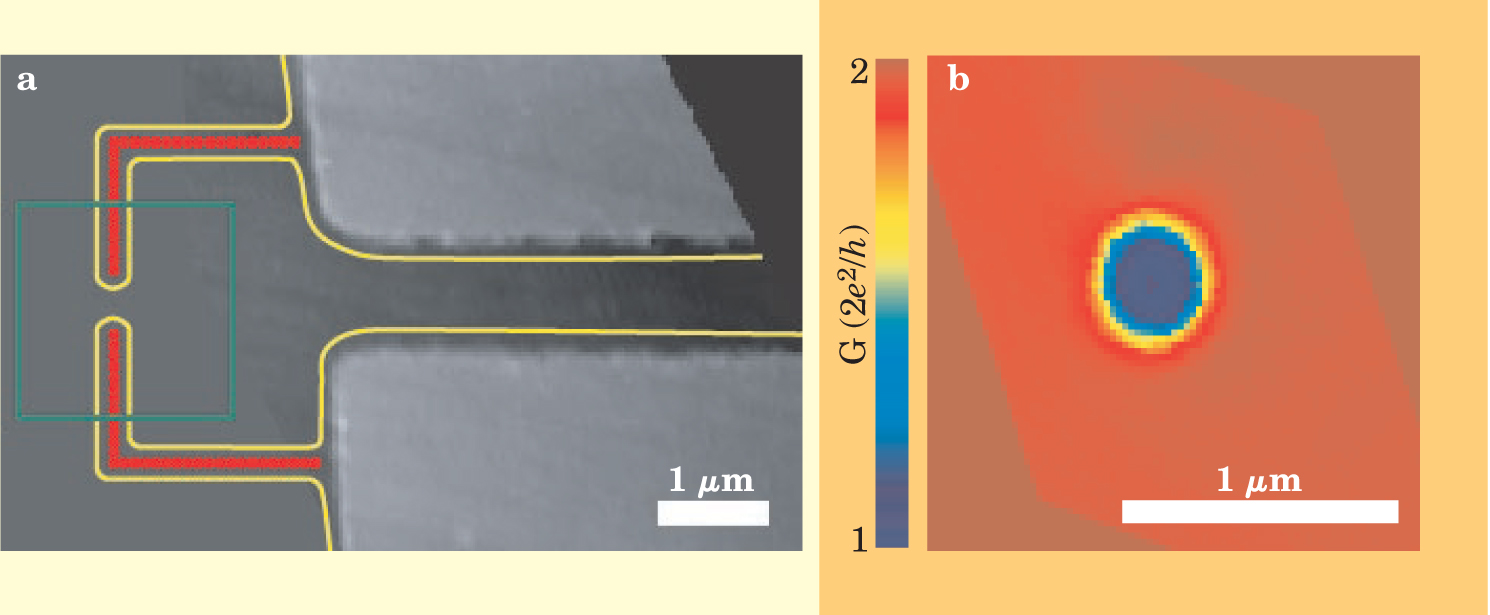
Raymond Ashoori’s group at MIT has developed a way to image electron flow in the quantum Hall regime using a subsurface charge accumulation (SCA) probe. 6 An STM tip held above the surface capacitively couples to the 2DEG immediately below. When a small AC voltage is applied between the tip and the 2DEG, the resulting flow of charge in the gas induces an oscillating image charge on the tip; that oscillation is detected by a sensitive electrometer. Adding a positive DC voltage to the tip allows spatial profiling of the 2DEG by creating a small bubble composed of a few electron charges beneath the tip. The bubble is surrounded by an insulating ring of incompressible fluid in the quantum Hall regime, and it forms an electrically isolated quantum dot that holds a fixed, discrete number of electron charges. 7
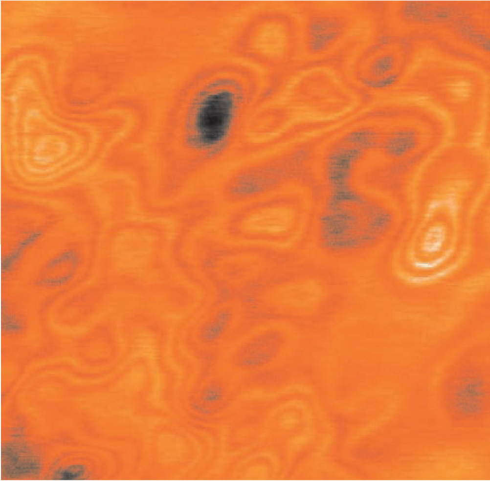
Figure 2 is an image of the SCA signal obtained as the bubble is moved through the 2DEG by scanning the STM tip above the surface. As the number of electrons in the bubble changes, the signal intensity oscillates, which results in bright strips that form a contour map of the random electrostatic potential inside the quantum Hall liquid. This image directly demonstrates how, thanks to the 2DEG’s incompressibility, the QHE can block the flow of electrons inside the electron gas.

Figure 2. Subsurface charge accumulation in a two-dimensional electron gas maps the electrostatic potential experienced by the 2DEG in the quantum Hall regime with a filling factor ν = 1. A positive voltage on the tip of a scanning tunneling microscope above the sample pulls in electrons to create a few-electron bubble in the 2DEG. The closed contours in this 2.5 × 2.5-µm2 image are caused by the quantization of electronic charge inside the bubble: The contours, which arise as individual electrons move in and out of the bubble, surround high and low regions of the random electrostatic potential.
(Adapted from ref. 7.)
Amir Yacoby (now at the Weizmann Institute of Science) and his colleagues at Lucent Technologies’ Bell Labs developed an alternate way to image the charge of an electron gas.
8
They successfully fabricated a single-electron transistor (SET) on the tip of a glass fiber and used it as a scanning electrometer probe. The SET was sensitive enough to detect changes in the 2DEG potential and density variations corresponding to tiny fractions of a single electron. With their probe, they imaged edge states that pass around the circumference of the electron gas in the quantum Hall regime (see figure 3(a)). The image was produced by measuring the charge induced on the SET electrometer when a voltage was applied to a gate electrode beneath the 2DEG. The incompressible strips of electron gas next to the edge states allowed the electric field to pass through the 2DEG to reach the SET; the result was the bright strips in figure 3(a). The SET tip was also used to image the Hall potential, as shown in figure

Figure 3. Imaging with a single-electron transistor. (a) Edge states form along the boundaries of a two-dimensional electron gas in the quantum Hall regime. The bright strips in this 15 × 15-µm2 image are incompressible regions of the electron gas next to the edge state for a filling factor ν = 2. The incompressible regions allow the electric field from an electrode beneath the 2DEG to reach the SET. (Negative voltage applied to the two black gate electrodes has closed the constriction between them.) (b) The SET probe can also detect changes in potential. A current flowing through an open aperture between the electrodes generates a transverse Hall potential that appears along the edges of the electrodes. No longitudinal potential is apparent at the top and bottom of this 7 × 7-µm2 image.
(Adapted from ref. 8.)

The quantum Hall regime imaging by the MIT and Bell Labs teams—as well as by Paul McEuen 10 at the University of California, Berkeley and Cornell University, by Jürgen Weis and Klaus von Klitzing 11 at the Max Planck Institute for Solid State Research in Stuttgart, Germany, and by Klaus Ensslin 12 at ETH Zürich—represents groundbreaking achievements that have enriched theories of the QHE and revealed intriguing new effects.
Imaging electron flow in low magnetic fields
Although many insights have come from imaging the quantum Hall regime, the majority of semiconductor devices operate without an applied magnetic field, making it important to image in that regime, too. Recent imaging by our group at Harvard University, by McEuen, by Charles Smith and David Ritchie at the University of Cambridge, and by Ensslin has focused on electron flow patterns in a 2DEG with no applied magnetic field or with small magnetic fields. Mark Eriksson, working with two of us (Topinka and Westervelt), led the charge in 1996 by directly imaging the mean free path in a 2DEG for electrons passing through a wide constriction. 13 Four years later, Rolf Crook and colleagues at Cambridge imaged cyclotron orbits in a 2DEG at 4.2 K and interpreted features of their images in terms of the deflections in electron trajectories caused by donor atom density fluctuations and impurities. 14 Using a charged atomic-force microscope tip to bend the trajectories of electrons traveling between two QPCs, they achieved glimpses into the spatial details of electron flow in 2DEG nanostructures. Those early experiments set the scene for more recent high-resolution images that revealed surprising and important details about electron flow in 2DEGs.
At Harvard, we used scanning probe microscopy to image the coherent flow of electron waves through a 2DEG with no applied magnetic field. 15,16 We focused on the pattern of electron flow through one of the most fundamental and widely used nanostructures: a QPC, 17 a narrow constriction whose width is comparable to the electrons’ Fermi wavelength λF (see Physics Today, July 1996, page 22 ). As its width is increased, the conductance of a QPC increases in steps of height 2e 2/h because the electrons travel through individual transverse modes, each of which contributes 2e 2/h to the total conductance.
Figure 4(a) illustrates our technique for imaging the flow of electron waves in a GaAs–AlGaAs 2DEG. Gates on the surface form a QPC whose width could be adjusted by changing the gate voltage. A charged SPM tip capacitively couples to the electron gas below; for negative tip-to-gas voltages, it can deplete a small, round divot in the 2DEG that reflects electron waves arriving from the QPC. The pattern of electron waves scattered by the divot under the tip is shown by theoretical simulations in the figure. Some of the electrons reflected by the divot return along their incoming path and travel back through the QPC, measurably reducing its conductance. Electrons scattered at other angles have little effect on the conductance because they remain on the same side of the QPC. The change in conductance induced by the tip is proportional to the flux of electrons hitting the divot under the tip. As the tip is scanned over the sample, the QPC conductance images the electron flux that was there before the tip was present.

Figure 4. Electron flow through a quantum point contact. (a) Scheme for imaging current flow through a QPC using scanning probe microscopy. Two gate electrodes (yellow) create a narrow constriction in the underlying two-dimensional electron gas. A charged tip (green) depletes the electron gas below it, creating a divot (red spot) that scatters incoming electron waves, as shown in the simulations (blue). (b) The conductance of the QPC, measured at 1.7 K, increases in quantized steps as the gate voltage (and QPC width) is increased. The insets below each step show simulations of the spatial pattern of electron flow for the transverse modes that contribute to the conductance. (c–e) Experimental images of electron flow at 1.7 K (left and right) and theoretical simulations (center) for the first three transverse modes of a QPC. The observed interference fringes spaced by half the Fermi wavelength demonstrate the coherence of electron flow. Because the additional flow, appearing as the QPC becomes wider, is due to the newly opened-up mode, the image for each transverse mode could be obtained by subtracting the raw images from the next lower step.
(Adapted from ref. 15.)
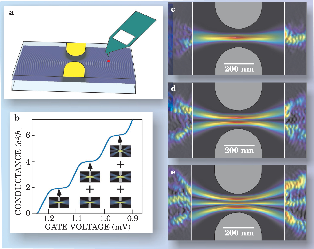
With this technique, we could image the patterns of electron flow through the individual transverse modes of the QPC that are responsible for the conductance steps shown in figure
The spatial resolution of the images in figure
At greater distances from the QPC, we discovered that the electron flow formed remarkably narrow branches, as shown in figure 5 for the first QPC conductance step.
16
From the experimental images and simulations close to the QPC shown in figure

Figure 5. Electron flow through a two-dimensional electron gas from a quantum point contact on the first conductance step. The image shows surprisingly narrow branches that are produced by small-angle scattering from charged donor atoms in the donor layer, as shown in figure
(Adapted from ref. 16.)

The formation of branches is a generic feature of electron flow in a 2DEG and is associated with small-angle scattering of electrons by the random potential induced by ionized donor atoms in the donor layer (see figure 1). In macroscopic measurements of the conductance, the electron diffusion constant in 2DEGs at low temperatures is determined by small-angle scattering. As shown in figure 1, the scattered electrons travel along smoothly curved paths rather than straight lines. Because the positions of the ionized donors remain fixed at low temperatures during the time required to record an image, these curved paths can be visualized. Thus one can image spatial structures, like the branches in figure 5, that would not be visible in an ensemble average over many samples.
Ray-tracing simulations of the classical trajectories for electrons in an accurate depiction of the potential landscape in the 2DEG gives results like figure 6(c), which shows a branching structure similar to the experiments. 16 Branches are also clearly seen in this month’s cover image, which shows the simulated paths of 50 000 electron trajectories.

Figure 6. Simulations of electron flow. (a) Parallel electron trajectories, going from left to right, form a V-shaped cusp due to focusing by a potential-energy dip caused by a charged donor atom (not seen) above a two-dimensional electron gas. (b) A realistic 2DEG simulation that includes many ionized donors forms several generations of cusps. The electrons travel here from upper left to lower right. (c) Ray-tracing simulations of electron flux emerging from a small opening into a region of random potential reflect the features seen in experimental images of 2DEG quantum point contact samples. The potential is shown green in the valleys and white on the peaks. The electron flux is coded by height and color, with blue corresponding to regions of low flux; still lower flux is transparent. The “shadow” of the flux on the potential plot shows where the flux lies relative to the hills and valleys; no guiding valleys are seen. A slight change of the position of the opening changes the location and direction of the branches.
(S. E. J. Shaw, PhD thesis, Harvard University, 2002.)
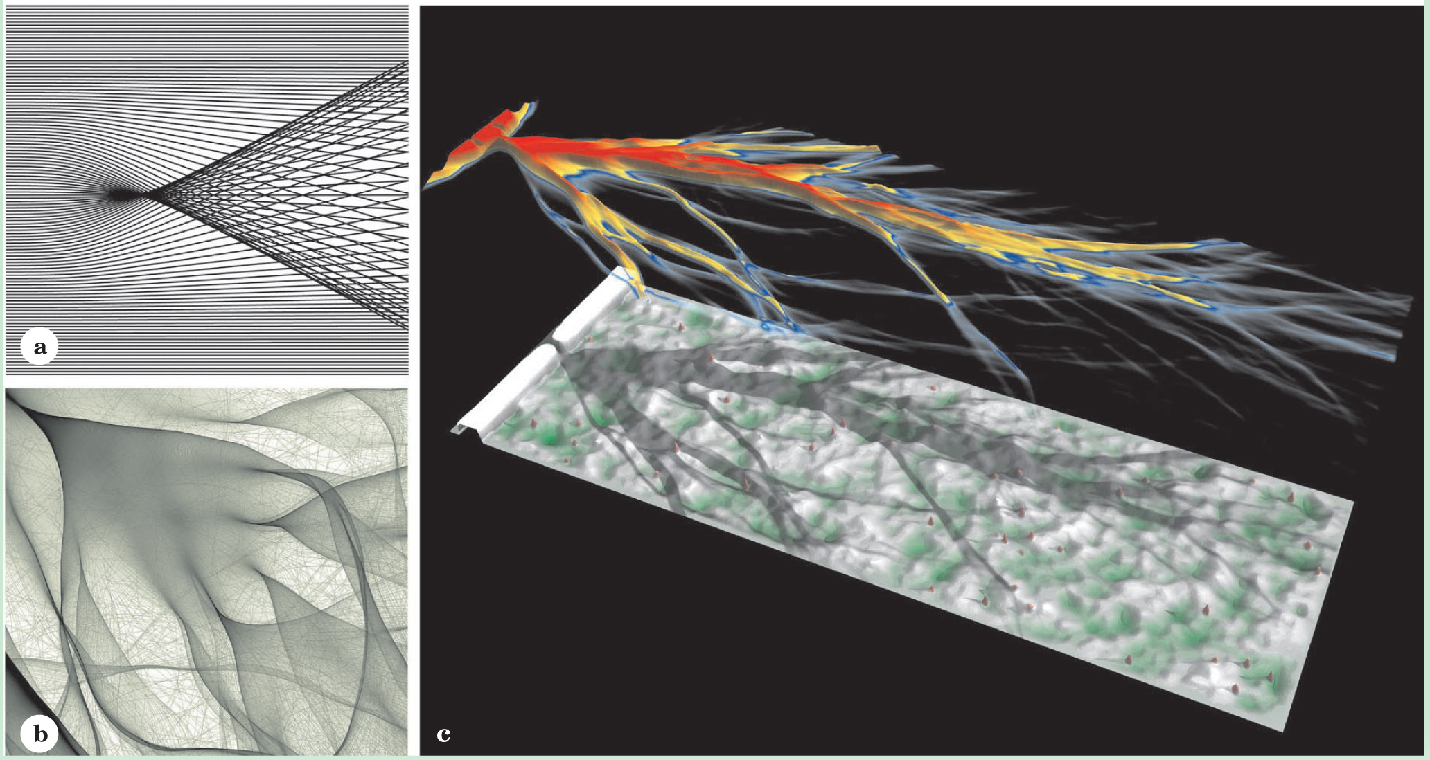
Closer inspection of the ray-tracing simulations reveals a lensing effect that, in hindsight, might have been expected. The hills and dales in the effective potential through which the electrons in the 2DEG pass deflect the electrons this way and that, occasionally inducing V-shaped cusps in the flow that correspond to folds in the position and momentum phase space for electrons. The simulation in figure
An imaging revolution
New ways to form and image quantum structures are developing rapidly. For example, Smith and Ritchie recently used an SPM tip to produce quantum structures in a 2DEG with erasable electrostatic lithography. 18 In that technique, an SPM tip is used to deposit charge on the surface of a heterostructure at low temperatures. Negative charge tends to deplete the underlying 2DEG and oppose the flow of electrons, and thus it creates the walls for a quantum structure. Figure 7 shows the location of the deposited charge defining a QPC; a conductance dip observed when the charged SPM tip is scanned above the QPC confirms the QPC’s location. Erasable lithography provides a new ability to change the geometry of a quantum structure during an experiment.

Figure 7. Erasable electrostatic lithography can fabricate customized two-dimensional electron gas devices. (a) A scanning probe microscope tip held at a negative voltage has deposited dots of charge (red) on the surface above a 2DEG. The deposited charges, along with fabricated electrodes (gray), define the walls of the 2DEG structure (yellow). (b) As the charged SPM tip is scanned above the area outlined in green in panel (a), the conductance of the 2DEG shows a dip when the tip is over the quantum point contact defined by the deposited charge.
(Adapted from ref. 18.)
The success that a number of groups have had in imaging the flow of electrons—the lightest by far of all the easily accessible particles—through a 2DEG involves a subtle change of mindset, away from the ensemble and toward the individual. In condensed matter physics, there is a strong tradition of considering ensemble averages, but now researchers are increasingly confronted with a specific quantum structure, with all its warts and bumps. For example, the branching of electron flow in 2DEGs is entirely consistent with earlier work using macroscopic measurements of conductance. But the newly discovered branches put a face on the real agent of momentum decorrelation and even tell where donor atoms may be located in a particular sample.
References
1. T. Chakraborty, P. Pietilainen, eds., The Quantum Hall Effects: Integral and Fractional, 2nd ed., Springer-Verlag, New York (1995).
2. L. L. Sohn, L. P. Kouwenhoven, G. Schön, Mesoscopic Electron Transport in Semiconductor Nanostructures, Kluwer Academic, New York (1997).
3. K. K. Likharev, Proc. IEEE 87, 606 (1999) https://doi.org/10.1109/5.752518 .
4. S. A. Wolf, D. D. Awschalom, R. A. Buhrman, J. M. Daughton, S. von Molnar, M. L. Roukes, A. Y. Chtchelkanova, D. M. Treger, Science 294, 1488 (2001) https://doi.org/10.1126/science.1065389 .
5. C. H. Bennett, D. P. DiVincenzo, Nature 404, 247 (2000) https://doi.org/10.1038/35005001 .
6. S. H. Tessmer, P. I. Glicofridis, R. C. Ashoori, L. S. Levitov, M. R. Melloch, Nature 392, 51 (1998) https://doi.org/10.1038/32112 .
7. G. Finkelstein, P. I. Glicofridis, R. C. Ashoori, M. Shayegan, Science 289, 90 (2000) https://doi.org/10.1126/science.289.5476.90 .
8. A. Yacoby, H. F. Hess, T. A. Fulton, L. N. Pfeiffer, K. W. West, Solid State Commun. 111, 1 (1999) https://doi.org/10.1016/S0038-1098(99)00139-8 .
9. N. B. Zhitenev, T. A. Fulton, A. Yacoby, H. F. Hess, L. N. Pfeiffer, K. W. West, Nature 404, 473 (2000) https://doi.org/10.1038/35006591 .
10. K. L. McCormick, M. T. Woodside, M. Huang, M. Wu, P. L. McEuen, C. Duruoz, J. S. Harris Jr, Phys. Rev. B 59, 4654 (1999) https://doi.org/10.1103/PhysRevB.59.4654 ;
M. T. Woodside, C. Vale, P. L. McEuen, C. Kadow, K. D. Maranowski, A. C. Gossard, Phys. Rev. B 64, 041310 (2001) https://doi.org/10.1103/PhysRevB.64.041310 .11. P. Weitz, A. Ahlswede, J. Weis, K. v. Klitzing, K. Eberl, Physica E 6, 247 (2000) https://doi.org/10.1016/S1386-9477(99)00136-8 ;
E. Ahlswede, P. Weitz, J. Weis, K. v. Klitzing, K. Eberl, Physica B 298, 562 (2001) https://doi.org/10.1016/S0921-4526(01)00383-0 .12. T. Ihn, J. Rychen, T. Vancura, K. Ensslin, W. Wegscheider, M. Bichler, Physica E 13, 671 (2002) https://doi.org/10.1016/S1386-9477(02)00255-2 .
13. M. A. Eriksson, R. G. Beck, M. A. Topinka, J. A. Katine, R. M. Westervelt, K. L. Campman, A. C. Gossard, Appl. Phys. Lett. 69, 671 (1996) https://doi.org/10.1063/1.117801
14. R. Crook, C. G. Smith, M. Y. Simmons, D. A. Ritchie, Phys. Rev. B 62, 5174 (2000) https://doi.org/10.1103/PhysRevB.62.5174 .
15. M. A. Topinka, B. J. LeRoy, S. E.J. Shaw, E. J. Heller, R. M. Westervelt, K. D. Maranowski, A. C. Gossard, Science 289, 2323 (2000) https://doi.org/10.1126/science.289.5488.2323 .
16. M. A. Topinka, B. J. LeRoy, R. M. Westervelt, S. E. J. Shaw, R. Fleischmann, E. J. Heller, K. D. Maranowski, A. C. Gossard, Nature 410, 183 (2001) https://doi.org/10.1038/35065553 .
17. B. J. van Wees, H. van Houten, C. W.J. Beenakker, J. G. Williamson, L. P. Kouwenhoven, D. van der Marel, C. T. Foxon, Phys. Rev. Lett. 60, 848 (1988) https://doi.org/10.1103/PhysRevLett.60.848 ;
D. A. Wharam, T. J. Thornton, R. Newbury, M. Pepper, H. Ahmed, J. E.F. Frost, D. G. Hasko, D. C. Peacock, D. A. Ritchie, G. A. C. Jones, J. Phys. C 21, L209 (1988) https://doi.org/10.1088/0022-3719/21/8/002 .18. R. Crook, A. C. Graham, C. G. Smith, I. Farrer, H. E. Beere, D. A. Ritchie, Nature 424, 751 (2003) https://doi.org/10.1038/nature01841 .
More about the authors
Mark Topinka, now an Urbanek Postdoctoral Fellow in the applied physics department at Stanford University, received his PhD from Harvard University under Bob Westervelt, Mallinckrodt Professor of Applied Physics and of Physics. Rick Heller is a professor of chemistry and physics at Harvard.
Mark A. Topinka, 1 Stanford University, US .
Robert M. Westervelt, 2 Harvard University, US .
Eric J. Heller, 3 Harvard University, US .


