Fifty years of seeing atoms
DOI: 10.1063/1.2195313
In a couplet nearly two and a half millennia ago, the Greek philosopher Democritus theorized the existence of atoms as the fundamental unit of matter: “By convention sweet, by convention bitter, by convention hot, by convention cold, … but in reality atoms and void.” Proving the hypothesis has taken a while.
Modern atomic theory began in 1803 when John Dalton first linked the notion of atoms with the concepts of stoichiometry and chemical reaction. Jean-Baptiste Perrin then affirmed the theory in 1905 when he obtained Avogadro’s number from a study of Brownian motion. And Max von Laue in 1912 used x-ray diffraction to show that a crystal was a periodic array of atoms. Encouraged by the evidence, albeit indirect, scientists tried to see atoms directly by using microscopy. The effort took half of the 20th century.
Last October marked the 50th anniversary of the first direct observation of atoms. In 1955, working in a dark room at the Pennsylvania State University with the field-ion microscope (FIM) he invented in 1951, 1,2 Erwin Müller and his student Kanwar Bahadur were able to make out the faint glow of helium ions as they hit a phosphorous screen and projected a highly magnified image of the arrangement of tungsten atoms on the surface of a sharp needle. Figure 1(a) shows a modern FIM atomic image. To commemorate the historic occasion, Allan Melmed of NIST, Imago Scientific Instruments Inc director Thomas Kelly, and Michael Miller of Oak Ridge National Laboratory organized two symposia last summer—one at the 2005 Microscopy and Microanalysis conference 3 in Hawaii, the other at Penn State.

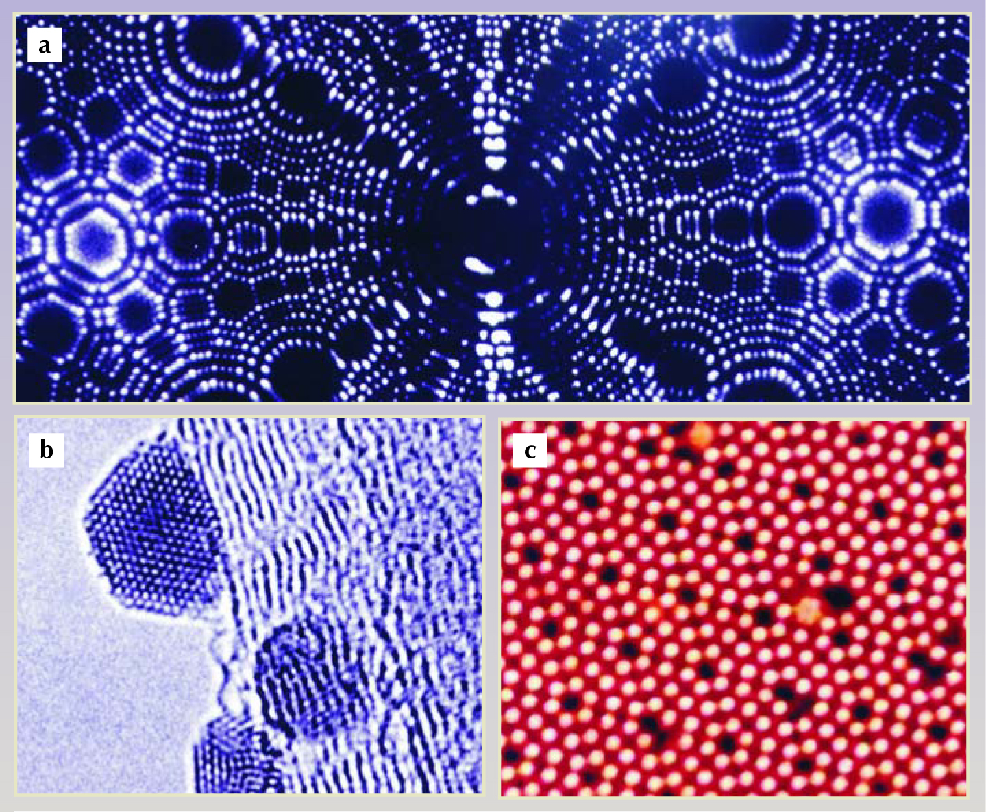
Figure 1. A gallery of atomic images. (a) This field-ion microscope image reveals the arrangement of atoms on a sharp tungsten tip. Each bright spot represents an atom or, more accurately, the impact of about 1000 helium ions accelerated in a radial direction from an atom at the tip’s surface. The tip’s hemispherical structure, basically a stack of circular atomic layers, accounts for the ringlike structure and many facets evident in the image. (b) Transmission electron microscopy effectively produces a shadow by scattering an electron beam as it passes through a thin sample. Dark spots represent columns of atoms in the lattice, silver nanocrystals grown in this case on a multiwall carbon nanotube. The parallel lines represent the layered inner wall of the nanotube. (c) This scanning tunneling microscope image illustrates the 7 × 7 reconstruction of silicon’s densest surface plane. The atomic image is a three-dimensional record of differences in the height of a metallic tip whose tunneling current into the surface is held constant by a feedback loop as the tip scans horizontally across the sample. Atomic defects and clusters are visible within the otherwise ordered plane.
The long journey
Much of scientists’ excitement over Müller’s achievement arose from the nature of the evidence it provided: visual proof. In the form of a magnified image, such proof can be the most convincing kind. The technology for making lenses to see things dates back to the Vikings and the Arabs in the 10th century, though Galileo is among the first to have used telescopy in the early 17th century, most famously to observe hills and valleys on the Moon and discover the four satellites of Jupiter. The single-lens optical microscope dates back to the mid-15th century, and Antonie van Leeuwenhoek discovered microorganisms with one around 1674—the birth year of microbiology.
Zacharias Janssen constructed the first compound optical microscope in 1590. Even with improvements from Christiaan Huygens, Robert Hooke, and many others, the microscope still had a spatial resolution limited by lens aberrations and wave-diffraction effects to about 3000 Å. Atoms are a thousand times smaller than that.
Shortly after 1926, when Clinton Davisson, Lester Germer, and George Thomson experimentally confirmed Louis de Broglie’s revolutionary idea of matter waves, scientists realized that shorter-wavelength electrons could be used to lower the diffraction limit. One could simply replace a light beam with an electron beam, and optical lenses with electromagnetic ones. In 1931, Max Knoll and Ernest Ruska built the first transmission electron microscope (TEM). Their instrument fell short of reaching atomic resolution mainly because of lens aberrations. But today, technology that corrects spherical aberration allows researchers using a TEM to routinely achieve atomic resolution (see figure
Simply stated, the TEM scatters electrons from a properly tilted thin-film sample to reveal columns of atoms in the lattice. Single atoms can also be seen in special cases without the need for aberration corrections. For instance, Sumio Iijima, Kunio Takayanagi, and their colleagues recently imaged single gold atoms from a nanowire and atoms encased inside a carbon nanotube. And Albert Crewe, using a scanning TEM in 1969, saw thorium atoms sparsely adsorbed on a thin carbon film. 4 Electron microscopes of all types are now important tools for advanced research in materials and biological sciences.
Just six years after Knoll and Ruska’s achievement, Müller built a new kind of microscope—the field-emission microscope. 5 A high negative voltage applied to a sharp tip prompted electrons to tunnel out of the tip and follow a nearly radial path to a surrounding spherical phosphor screen. Thus, the image was an electron emission map of the tip’s surface, magnified by an amount around R/r—on the order of 105 to 106—where R is the distance from the tip to the fluorescent screen and r the tip’s radius of curvature. The variations in image intensity reflected the variations in the work function of the surface. Whereas surface diffusion of an adsorption layer was visible, the spatial resolution was limited to only about 20 Å because of electron diffraction. Although this resolution limit precluded seeing surface atoms, field emission still provides an electron source in many practical applications, often using tungsten tips coated with zirconium oxide.
To reduce the diffraction effect, Müller replaced electrons with heavier-mass atoms in 1951 while working at the Fritz Haber Institute in Berlin, Germany. 1 It occurred to him that he could adsorb hydrogen on the tip surface and then simply use a high positive voltage to desorb those atoms and achieve the same radial magnification with greatly improved resolution. The first field-ion microscope could see ring-shaped atomic steps with their edges often decorated with isolated spots, presumably adsorbed atoms. Improvements to the technology soon followed. He and Robert Gomer later realized that cooling the tip should reduce the thermal kinetic energy of desorbing atoms.
Moreover, a deeper theoretical understanding led Müller, by 1952 at Penn State, to conclude that images were formed by field ionization of hydrogen gas atoms hopping around the tip. Helium, inert and having a higher ionization field that could improve image resolution, then became the preferred image gas. 2 (See my earlier article in Physics Today, May 1993, page 24 .) In 1955, Müller and Bahadur built a cold finger for cooling the tip, and on 17 October they raised the voltage high enough so that field evaporation of adsorbed atoms and protrusions would smooth the tungsten emitter surface. To their great excitement they saw a markedly improved field-ion image whose atomic arrangement reflected the tungsten emitter surface—the historic first sighting of atoms.
From field emission to tunneling microscopy
Using a different approach to imaging, in 1971 Russell Young of the National Bureau of Standards (now NIST) developed a new kind of microscope called a topografiner (see his Physics Today article, November 1971, page 42 ). Young attached a sharp field-emission tip to the vertical, z-leg of a piezoelectric-controlled tripod. Electronic feedback kept the tip-to-sample distance constant by repeatedly monitoring the field-emission current between the two for a given tip–sample bias as the surface moved laterally underneath. The voltage difference applied to the z piezoelectric then represented the height of the surface as the tip was scanned in the other two dimensions using x and y piezoelectrics.
Using the setup, Young was able to draw a three-dimensional contour of the surface. He studied vacuum tunneling of electrons from the tip to surface, but published only topographic scans taken using field emission.
In 1983, IBM Zurich Research Lab’s Gerd Binnig and Heinrich Rohrer succeeded in imaging the elusive atomic arrangement of the 7 × 7 reconstruction of silicon(111) using a similar scanning device. Their scanning tunneling microscope (STM) worked in the vacuum-tunneling regime; it achieves atomic resolution because its tunneling current is so exquisitely sensitive to the slightest variation in tip–surface distance. In today’s STMs, piezoelectric motors allow the tip to trace out the atomic-scale surface topography while a computer records the 3D data.
6
An advantage of STM imaging, moreover, is that samples can be imaged not just in vacuum but also in ambient atmosphere, and samples are not required to be sharply pointed needles. Figure
Instead of sensing the tunneling current, one can also sense the force acting between atoms of the sample and those in the tip. Such atomic force microscopes (AFMs) are particularly well suited to imaging materials of poor electrical conductivity at the atomic scale and biological molecules. 7 But many other variations are possible, including magnetic force microscopes that image a material’s spin configurations and near-field scanning optical microscopes that radically improve the diffraction limit. The many versions of scanning probe microscopes (SPMs) can be used not only for atomic-resolution studies of materials but also for measuring, with great sensitivity, many diverse physical properties of nanostructures.
Seeing surface atoms
After achieving atomic resolution, Müller immediately applied the FIM to observe defects of metals created by α-particle bombardment. During the 1960s and early 1970s, he continued to improve the technology’s instrumentation and image-formation mechanism. Going beyond its use as a tool to study fundamental surface phenomena, engineers and scientists in major university, industrial, and government laboratories around the world applied the FIM to metallurgy and materials science.
Three atomic processes are responsible for forming field-ion images. 2 As the positive applied tip voltage gradually increases, atoms on the tip start to evaporate one by one in the form of ions. This field evaporation occurs at asperities and step edges where local fields are highest, a process that smooths the surface. Attracted to the emitter surface by the field-induced polarization force, image-gas atoms—usually helium or neon—are adsorbed atop surface atoms. The hopping inert gas atoms are ionized by the electric field at a critical distance above the tip in a disk-shaped ionization zone only about 0.2 Å in thickness. The ions then gain up to 20 keV in kinetic energy as they are accelerated from the hemispherical tip surface to the phosphor screen, where they form a projection image.
The high spatial sensitivity of electron tunneling in field ionization is similar to the vertical sensitivity of electron tunneling in an STM. 8 The image-gas atoms hop around the tip surface by virtue of the field gradient near it. But lateral motion of those gas atoms limits the FIM resolution. Using a cold finger to cool the tip also cools the hopping gas atoms and thereby minimizes the lateral velocity spread of the ions and improves the instrument’s spatial resolution.
For a material to give rise to a good FIM image, its evaporation field has to be close to or higher than the best image field of the image gas. The best image field of helium is about 4.5 V/Å, and for neon about 3.8 V/Å. The field requirement limits the material applicability of the FIM. With patience, however, one can resolve good images of even such soft metals as aluminum and gold. 2
Some of the most important applications of field-ion microscopy are in metallurgy. Although the hemispherical shape of the tip surface makes detailed image analysis difficult, researchers have studied atomic structures and impurity-segregation phenomena—including grain-boundary segregations, precipitate formation, decomposition of alloy species, and a host of others—in atomic detail at various lattice defects. 2
Applications to surface physics include the study of thermal diffusion of single surface atoms, their mutual interactions, and the mechanisms and energetics of atomic processes. Details about those processes contribute to the fundamental understanding of epitaxial growth of thin films. Since 1966 Gert Ehrlich and coworkers have studied the random diffusion of single metal adatoms on metal surfaces. 9 In addition to deriving diffusion parameters, they found that diffusing adatoms were reflected at surface steps. Indeed, distinct modes in thin-film growth can be understood as a result of the barrier height of such steps.
Adsorbed atoms usually move by hopping from one point on the surface to another, but on surfaces of some face-center-cubic metals, adatoms can move by simply exchanging positions with atoms in the lattice. Researchers use STM routinely to study diffusion of single atoms, atomic clusters, and various molecules on metal and semiconductor surfaces. 10
Atomic interactions and their collective effects govern the physical world. In 1972 I published an FIM study of atomic interactions that emphasized control over the number of atoms adsorbed on a facet of the tip. 11 The experiment traced the movement of each adatom while clusters were built up atom by atom in a way similar to the bottom-up approach often used in nanotechnology today. The pair potential between two rhenium atoms on the tungsten(110) surface was found in the experiment to have at least two minima and one maximum, a result that suggested an oscillatory structure similar to the so-called Friedel oscillations of impurity-atom interactions inside metals. (For other examples of the interference effects from the presence of impurity atoms, see figure 2.) The pair interaction can now be derived by measuring the 2D pair distribution, or by observing the frequency at which different cluster configurations appear. With computer image digitizers now widely available, the adatom–adatom interaction and surface potential seen by a diffusing atom can be studied quantitatively using an FIM and STM and compared with theories derived from first principles. 12

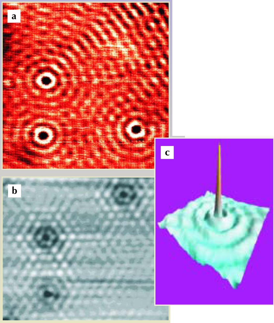
Figure 2. A scanning tunneling microscope (STM) image is a map of the electronic density of states of the surface. (a) Electrons scattered by three impurity atoms, imaged as dark depressions, produce wave-interference patterns on the copper(111) surface. (b) A monolayer of lead is grown over a 1 × 1 surface of silicon(111). As imaged by an STM, the atoms rearrange to form a hexagonal ringlike corrugation because of indirect electronic interactions between lead atoms. (c) A three-dimensional perspective of the interference pattern formed around a cerium impurity on the (111) surface of silver. The rippled topography matches what is expected from a many-electron solution to the Schrödinger wave equation for the atomic configuration.
(Figure 2b adapted from I.-S. Hwang et al.,
Atoms subjected to an external force tend to move preferentially in the direction of the applied force, whether it comes from a long-range interaction between atoms or between an atom and a lattice defect like a step edge, or from an applied electric-field gradient. Using an FIM in 1971, Gary Kellogg and I directly observed and studied the directional walk of tungsten adatoms induced by an applied field gradient on the tungsten(112) and (110) surfaces. 13 Measuring the velocity of an adatom under an applied field gradient allowed us to derive the surface-induced dipole moment and polarizability of the adatoms.
Although it is not clear whether Müller’s 1955 achievement stimulated any of the ideas expressed in Richard Feynman’s famous lecture, “There Is Plenty of Room at the Bottom,” delivered at the 1959 Caltech meeting of the American Physical Society, the maturing of atomic-resolution microscopy did spur researchers to build artificial nanostructures atom by atom. In the early 1990s IBM’s Don Eigler and others demonstrated the dramatic use of scanning probe microscopy as a tool that can directly manipulate atoms (see figure 3). 14 Understanding the detailed atomic processes involved in such manipulation may indeed have accelerated the development of Masakazu Aono’s atom switch, an electrical device made from a cluster of fewer than a hundred silver atoms, 15 and similar atomic-scale devices.

Figure 3. Atomic manipulation. (a) A scanning tunneling microscope (STM) tip was used to construct a “quantum corral” from 48 iron atoms adsorbed on a copper(111) surface. How do the tip and surface atoms interact? Generally, an atom can be field-evaporated from a surface or pushed and pulled across it using the tip as a rake or shovel, but here a gentle voltage pulse applied to the tip induces the adsorption of an iron atom onto it. After the tip moves to some new location, another voltage pulse redeposits that atom to the surface. Scanning the electron densities on the surface at various stages of completion (clockwise from top left) records the progress (see the article in Physics Today,
(Images courtesy of D. Eigler, S. Hosaka, and S. Morita.)
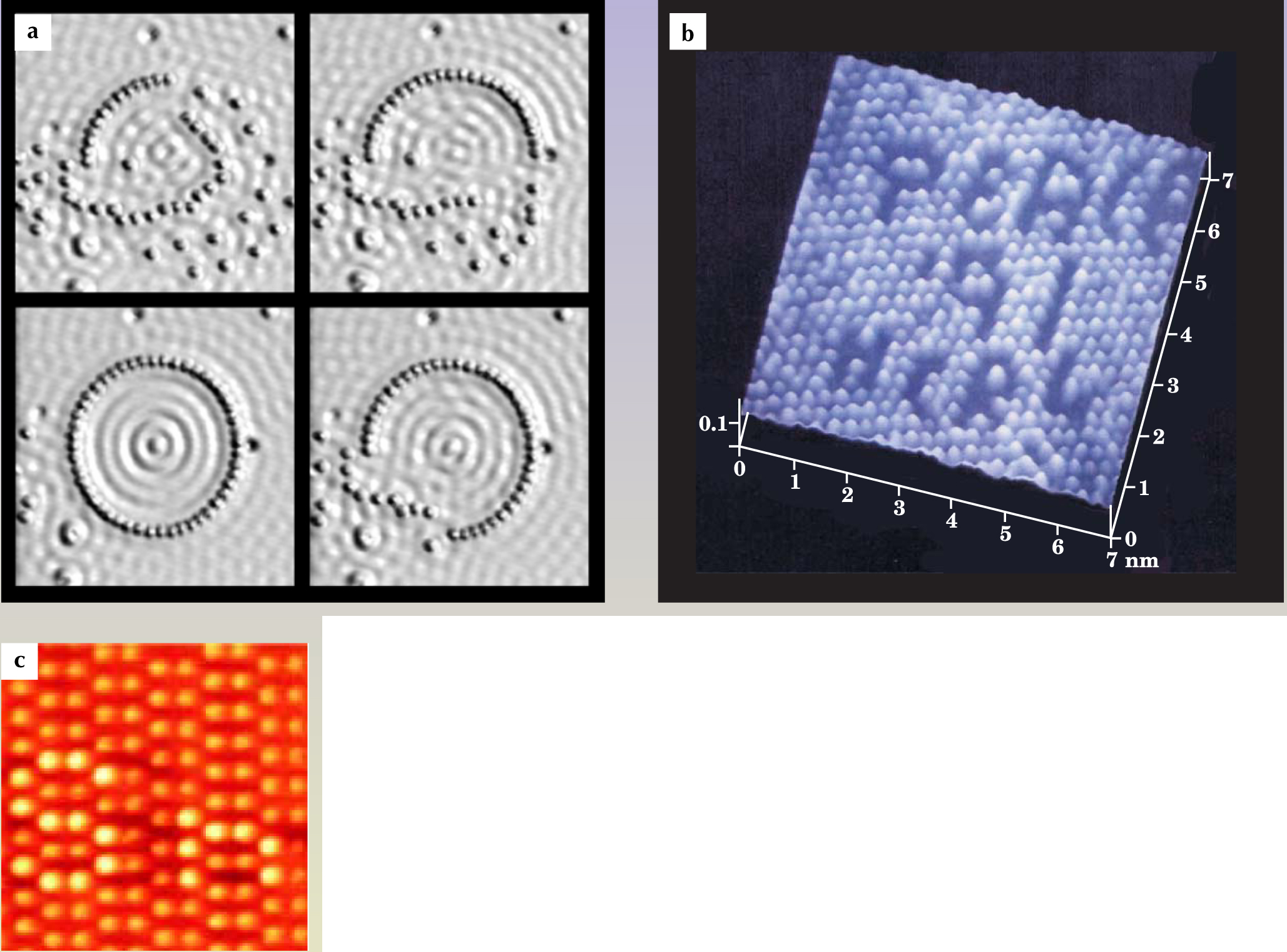
Artificially controlled movements and the transfer of atoms to intended points along the surface take the form of a directional walk induced by an attractive or repulsive atomic interaction—that is, by pulling or pushing a surface atom using atoms of the probe tip. Alternatively, field evaporation by a voltage pulse from the tip can make the tip adsorb a surface atom, which can then be transferred to some other spot where a reverse-polarity pulse on the tip redeposits the atom.
Elemental mapping
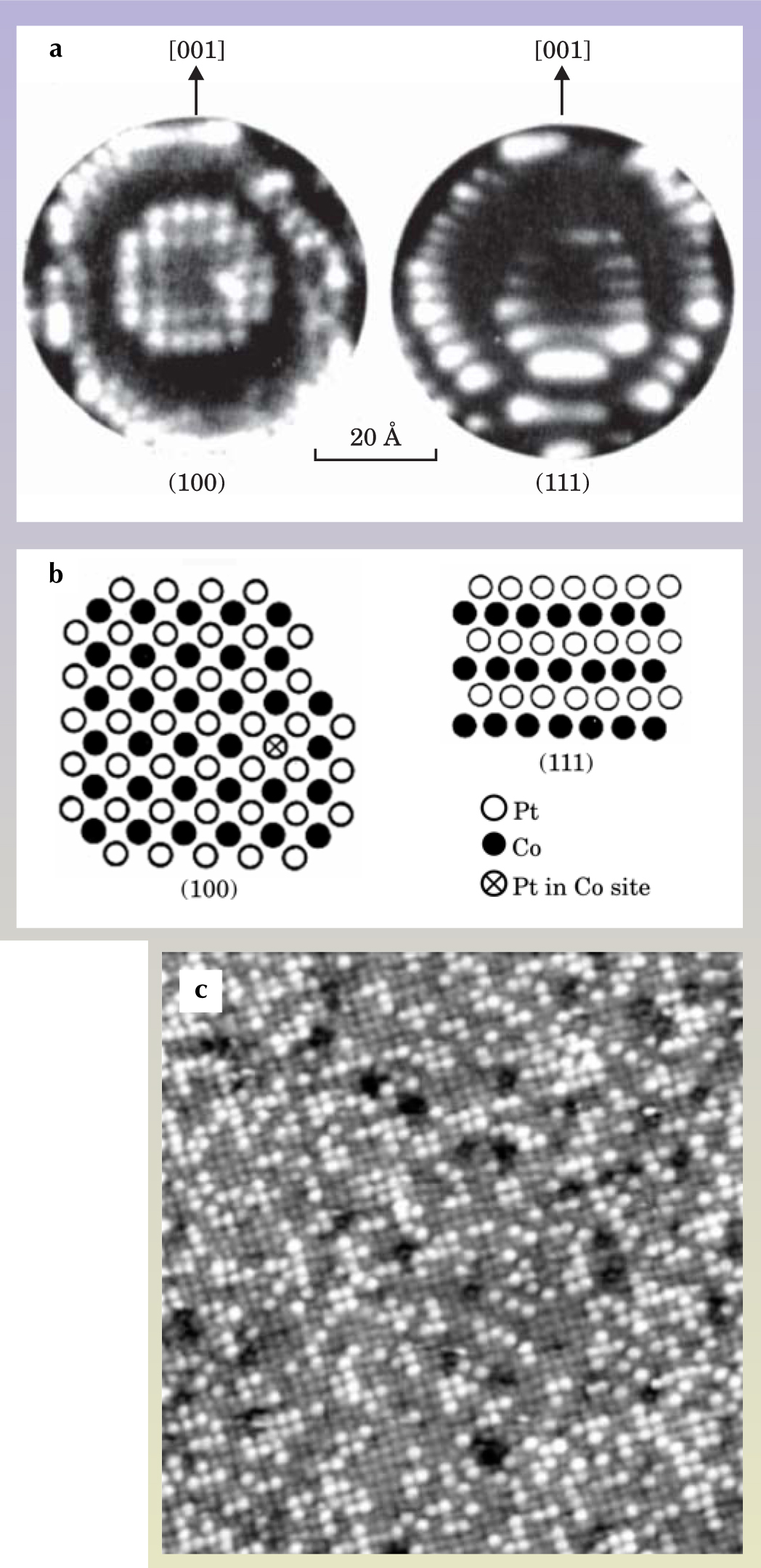
An important function of atomic-resolution microscopy is determining what elements are on the surface and where they are located. The earliest attempt focused on whether or not one species of an alloy could be distinguished from another in the resulting image. Müller and I used an FIM on ordered alloys in 1967 to demonstrate the chemical contrast. 2 In ordered platinum cobalt alloys, we noticed that only platinum atoms formed an image, a consequence of platinum having a higher field ionization than cobalt, whose atoms appeared so dim as to be nearly invisible.
Other ordered alloys such as nickel-containing tungsten or molybdenum compounds exhibited a similar effect: The nickel atoms appeared nearly invisible in the FIM image. Peter Varga and colleagues from the Technical University of Vienna reported a similar chemical contrast in scanning tunneling microscopy a quarter-century later in PtNi3 and PtRh alloys. As imaged by an STM, nickel and rhodium atoms appeared dimmer because of the smaller electronic density of states in those surface atoms. 16 The segregation of platinum from bulk layers of PtRh to the surface could then be mapped and studied by directly counting the number of platinum atoms in the STM image; the formation of clusters of atoms of the same species is, moreover, evident in the images (see figure 4).

Figure 4. Chemical maps of surface atoms. (a) In this platinum cobalt alloy, the ionization probability of helium above cobalt atoms is too low to render it visible in these field-ion microscope (FIM) images. Cobalt’s smaller size accounts for the smaller local field. Compared with the schematic view (b) of each atom in the (100) plane, the center of the experimental image, corresponding to the top layer of the tip, reveals only the square array of platinum atoms. Similarly, the FIM image of the (111) plane of PtCo alloy reveals only rows of platinum atoms. The circular rings in both images represent atoms located in the second layer. (c) In scanning tunneling microscopy, rhodium atoms appear dim compared to platinum atoms in PtRh metal alloys due to rhodium’s lower local electronic density of states.
(Figures 4a and 4b adapted from T. T. Tsong, E. W. Müller,
Until 1967, atomic-scale chemical mapping was not possible for materials of unknown composition. To solve the problem, Müller conceived the idea of atom-probe field-ion microscopy—a technique that combines FIM with time-of-flight mass spectroscopy. But rather than using noble-gas atoms to form an image, one keeps the instrument in vacuum and exposes the tip to a DC voltage plus a nanosecond voltage pulse, which field-evaporates sample atoms. Time-of-flight from the sample to detector yields the charge-to-mass ratio of those ions. A prototype linear atom-probe FIM was developed in 1967 and continuously improved with different designs. Using the time-of-flight technique, atoms of any mass could be detected. Nevertheless, early instruments suffered from poor mass resolution due to the large spread in ion energies caused by the high-voltage pulse during field evaporation. Incorporating an energy compensator into the design solved the dispersion problem. 2
High-voltage pulsed atom probes have found many applications in materials analysis: One can monitor the surface segregation of elements in an alloy and determine the composition layer by layer during depth profiling, to list one example. The technique has established the odd oscillatory behavior of elements as they segregate in some alloys in near-surface layers and the preferential segregation of an alloy component and impurities to step edges and grain boundaries. Compared to results obtained with macroscopic techniques, atom-probe analyses do not depend on fitting data with theoretical models; the element maps are true depth profiles of a material’s composition.
Moreover, using the atom probe to observe the complexes that helium ions make with metal atoms and the distributions of those ionic charge states improves our understanding of field evaporation and field adsorption. Studying the temperature dependence of the probability of detecting the metal-helide ions—and associated adsorption-isotherm data—provides insight into field adsorption phenomena. Novel ionic species can be created by field desorption of adsorbed gases and may one day be used to study the formation of novel chemical species in interstellar space; particles of space dust are highly charged by the continual showering of high-energy photons and charged particles; in that environment both field adsorption and evaporation can occur.
Early atom-probe instruments collected atoms from a small surface area covered by a small probe hole. In 1973 John Panitz introduced a variation on the technique, whereby field-evaporated ions form an image of the surface in vacuum on a microchannel-plate ion detector; 17 thus, the technique provides the location of an atom at the tip and identifies its chemistry. It has since matured into a 3D imaging tool through the efforts of the groups of George Smith at Oxford University, Didier Blavette at the University of Rouen in France, and Kelly of Imago Scientific, using position-sensitive ion detectors. A modern version of the instrument, outlined in figure 5, maps the position of an atom, field-evaporated from one of possibly many sharp needles on the surface and then sent through a micron-sized probe hole to a sensitive, microchannel-plate ion detector.

Figure 5. Materials analysis. (a) The three-dimensional atom probe is a projection microscope that uses field evaporation to project surface ions onto a position-sensitive detector and a time-of-flight mass spectrometer that identifies them chemically. A high-voltage pulse applied to a microtip on the surface, usually machined to sharp points at various places of interest and held at cryogenic temperatures, stimulates field evaporation of surface atoms into ions, which pass into the micron-sized cone entrance along a radial path toward the detector. The microscope provides a 3D element map. (b) This color-coded image identifies the distribution of boron atoms that have segregated to the core of a line dislocation in aluminum. The dislocation, roughly perpendicular to the page, occurs within the outlined box, whose top reveals one more atomic layer (in yellow) than in the bottom.
(Courtesy of G. D. W. Smith and D. Blavette.)

As atomic layers are gradually removed during field evaporation, a 3D element distribution can be reconstructed with subnanometer spatial resolution from the location and sequence of ions detected. With today’s instruments, the speed of data collection is now as high as a million ions per hour, and nanostructures buried hundreds of atomic layers below the surface can be imaged and analyzed.
Nanosecond-long high-voltage pulses in field evaporation produce a large spread of ion energies that greatly deteriorates the mass resolution of the time-of-flight atom probe, a problem that is especially serious for the short flight path of a 3D atom probe. In addition, the use of high-voltage pulses restricts the technique to conductive samples. To overcome both problems, I proposed in 1978 that laser pulses could be used to produce the field evaporation. 2 Two years later, Kellogg and I used an imaging atom probe operated by nanosecond laser pulses to determine the mass spectrum of silicon. The field-evaporation rate could be controlled by varying the laser power and an applied voltage. The diffusion of surface atoms under pulsed-laser action could be seen if the laser power was intentionally raised. Indeed, picosecond and femtosecond laser pulses are now often used to study surface-atom dynamics and field evaporation. 2
A high-resolution pulsed-laser atom-probe developed at Penn State between 1982 and 1990 adopted a number of innovative design features: A fixed-position 500-µm-diameter local probe was used to reduce the evaporation voltage and create a field-free flight path for improving the mass resolution. Two orthogonal telescopes were used to align the tip and laser beam, with a translating lens added for fine-tuning. In 1993 Osamu Nishikawa developed a local-probe atom probe with a micron-sized hole for analyzing soft materials. The Penn State system also included a picosecond pulsed laser, a picosecond-resolution electronic timer, high-stability high-voltage power supply, and a precision voltmeter. With proper calibration, the mass spectrometer and ion-energy analyzer had single-ion sensitivity and a spectral linewidth resolution—m/Δm, where m represents an ion’s mass—of 50 000. Besides its application to nanoanalysis, researchers used the Penn State machine to study the formation of metal helides, novel ions and clusters, field-induced dissociation like the so-called Coulomb explosion of multiply charged ions, and many other ion-physics phenomena. 2 Pulsed-laser techniques are now common to all commercial atom-probe systems and appear to promise much wider materials applicability in the future.
The journey continues
Field evaporation using an atom-probe FIM allows researchers to probe the bulk of a material and reconstruct a 3D perspective of its chemical makeup. But the process also destroys those layers during analysis and is tedious because it requires that any surface area to be analyzed be fabricated into a tip sharp enough to sustain high electric fields. With a TEM, researchers can distinguish the chemical nature of an atom based on its characteristic x-ray emission, but again only when the sample is specially shaped to suit the technique.
With an STM, researchers must first characterize the probing tip before understanding the meaning of their images, inasmuch as STM image brightness reflects the density of states of both the sample atom and the scanning tip. 8 If the tip is atomically sharp, then measuring the density of states of the tip apex atom and the sample atom makes it possible to identify the chemical element of the sample atom. The job is then to compare the results with theoretical analyses or standard samples.
In a study designed to influence the chemical reactivity of a metal surface by changing its morphology on the nanometer scale, Rutgers University physicist Theodore Madey and his colleagues reported methods of creating faceted surfaces by heating them after deposition of another metal or adsorption of oxygen. The method is now used to create atomically sharp, thermally stable, and chemically inert pyramidal tips that can be repaired repeatedly by simple annealing (see figure 6). 18 Atomically sharp tips, when used as an ion source, are the smallest point sources that provide a brightness comparable to sources in focused-ion-beam devices now used for imaging and lithography. Such a tip can also be used as a high-brightness point source of coherent-wave electrons, a line of research pursued by Chuhei Oshima and his colleagues at Waseda University in Japan. Electron microscopes using such a source may give a holographic 3D image of the near-surface layers of a nanostructure.

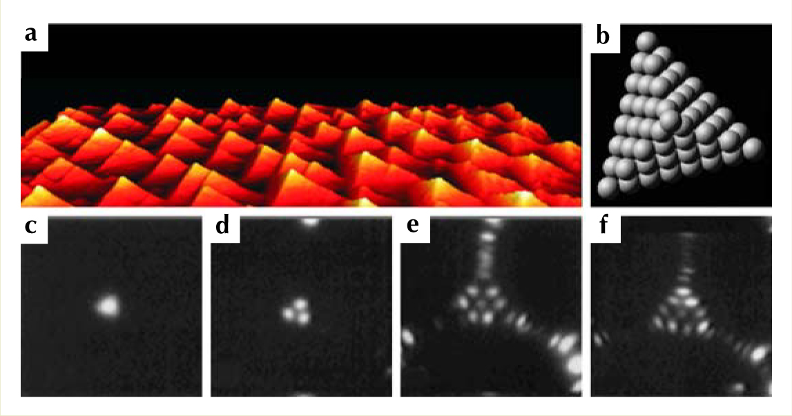
Figure 6. Creating sharp tips. (a) Heating an iridium surface covered with half a monolayer of oxygen to 1000 K can create a faceted surface like the one shown here, imaged using scanning tunneling microscopy. Such simple heating is one recipe for forming pyramidal nanostructures from a flat surface. (b) Atomic model of a tungsten tip oriented along the (111) plane and covered with a monolayer of adsorbed palladium atoms. (c–e) Field evaporation from a real tip reveals the first three atomic layers. The fact that the third layer (e) shows seven atoms instead of the ten expected from the model indicates the tip’s imperfection. (f) Heating the surface can repair a damaged or imperfect tip: Subsequent field evaporation now reveals an atomically perfect third layer.
(Figure 6a courtesy of I. Ermanoski and T. E. Madey
Atomic-resolution microscopy, in its various instrumental forms, is more than a set of imaging and chemical-analysis tools. The same principles that underlie the various instruments’ atomic-imaging ability can also be applied to making nanodevices and sensors with the sensitivity of a single atom or electron. Atomic-resolution microscopy is already finding applications in the form of nanomechanical resonators and sensors that use AFM cantilevers, radiofrequency amplifiers, and atomic switches (see the article by Keith Schwab and Michael Roukes in Physics Today, July 2005, page 36 ). We can surely expect more applications in the future.
I would like to thank coworkers Chia-Sen Chang, Ing-Shou Hwang, Wei-Bin Su, Tsu-Yi Fu, Mon-Shu Ho, and others at the Institute of Physics, Academia Sinica, as well as those who kindly prepared figures for this article.
References
1. E. W. Müller, Z. Phys. 131, 136 (1951).
2. E. W. Müller, T. T. Tsong, Field Ion Microscopy, Principles and Applications, Elsevier, New York (1969);
T. T. Tsong, Atom-Probe Field Ion Microscopy: Field Ion Emission and Surfaces and Interfaces at Atomic Resolution, Cambridge U. Press, New York (1990) https://doi.org/10.1017/CBO9780511599842 ;
M. K. Miller, A. Cerezo, M. G. Hetherington, G. D. W. Smith, Atom Probe Field Ion Microscopy, Oxford U. Press, New York (1996).3. Conference abstracts are available in Microsc. Microanal. 11, suppl. 1, 93 (2005).
4. A. V. Crewe, J. S. Wall, J. P. Langmore, Science 168, 1338 (1970) https://doi.org/10.1126/science.168.3937.1338 .
5. E. W. Müller, Z. Phys. 106, 541 (1937).
6. G. Binnig, H. Rohrer, C. Gerber, E. Weibel, Phys. Rev. Lett. 49, 57 (1982); https://doi.org/10.1103/PhysRevLett.49.57
G. Binnig et al., Phys. Rev. Lett. 50, 120 (1983) https://doi.org/10.1103/PhysRevLett.50.120 .7. G. Binnig, C. F. Quate, C. Gerber, Phys. Rev. Lett. 56, 930 (1986) https://doi.org/10.1103/PhysRevLett.56.930 .
8. J. Tersoff, D. R. Hamann, Phys. Rev. Lett. 50, 1998 (1983); https://doi.org/10.1103/PhysRevLett.50.1998
Phys. Rev. B 31, 805 (1985) https://doi.org/10.1103/PhysRevB.31.805 .9. G. Ehrlich, J. Chem. Phys. 44, 1050 (1966) https://doi.org/10.1063/1.1726788 .
10. J. V. Barth, Surf. Sci. Rep. 40, 75 (2000); https://doi.org/10.1016/S0167-5729(00)00002-9
I. S. Hwang et al., J. Phys. Chem. Solids 62, 1655 (2001) https://doi.org/10.1016/S0022-3697(01)00103-2 .11. T. T. Tsong, Phys. Rev. B 6, 417 (1972); https://doi.org/10.1103/PhysRevB.6.417
Rep. Prog. Phys. 51, 759 (1988) https://doi.org/10.1088/0034-4885/51/6/001 .12. M. L. Merrick, W. W. Luo, K. A. Fichthorn, Prog. Surf. Sci. 72, 117 (2003); https://doi.org/10.1016/S0079-6816(03)00020-0
F. Silly et al., Phys. Rev. Lett. 92, 016101 (2004) https://doi.org/10.1103/PhysRevLett.92.016101 .13. T. T. Tsong, G. L. Kellogg, Phys. Rev. B 12, 1343 (1975); https://doi.org/10.1103/PhysRevB.12.1343
S. C. Wand, T. T. Tsong, Phys. Rev. B 44, 13703 (1991) https://doi.org/10.1103/PhysRevB.44.13703 .14. D. M. Eigler, E. K. Schweizer, Nature 344, 524 (1990); https://doi.org/10.1038/344524a0
J. A. Stroscio, D. M. Eigler, Science 254, 1319 (1991); https://doi.org/10.1126/science.254.5036.1319
S. Hosoki, S. Hosaka, T. Hasegawa, Appl. Surf. Sci. 60-61, 643 (1992); https://doi.org/10.1016/0169-4332(92)90489-K
Y. Sugimoto et al., Nat. Mater. 4, 156 (2005) https://doi.org/10.1038/nmat1297 .15. K. Terabe et al., Nature 433, 47 (2005) https://doi.org/10.1038/nature03190 .
16. M. Schmid, H. Stadler, P. Varga, Phys. Rev. Lett. 70, 1441 (1993) https://doi.org/10.1103/PhysRevLett.70.1441 .
17. J. A. Panitz, Rev. Sci. Instrum. 44, 1034 (1973); https://doi.org/10.1063/1.1686295
J. A. Panitz, Prog. Surf. Sci. 8, 219 (1978) https://doi.org/10.1016/0079-6816(78)90002-3 .18. T. E. Madey et al., Proc. Nat. Acad. Sci. USA 99, 6503 (2002); https://doi.org/10.1073/pnas.062536499
T.-Y. Fu et al., Phys. Rev. B 64, 113401 (2002); https://doi.org/10.1103/PhysRevB.64.113401
H. S. Kuo et al., Nano Lett. 4, 2379 (2004) https://doi.org/10.1021/nl048569b .
More about the authors
Tien Tsong is a research fellow at the Institute of Physics, Academia Sinica in Taipei, Taiwan, and an emeritus professor of physics at the Pennsylvania State University.
Tien T. Tsong, Institute of Physics, Academia Sinica, Taipei, Taiwan .


