Atom-like crystal defects: From quantum computers to biological sensors
DOI: 10.1063/PT.3.2549


The idea that quantum mechanical machines can perform certain information-processing tasks much faster than any classical computer has captured the imagination of many people. That potential has led to a new era in quantum science, one in which researchers strive to identify and harness quantum systems and leverage them for computation, communication, sensing, and imaging. Two of the most promising platforms for reaching the coherence needed to achieve such goals are isolated atoms and solid-state devices. Ions and neutral atoms can be trapped using electromagnetic fields in high vacuum, which insulates them exceptionally well from noise. And their electronic states can be precisely controlled with optical, microwave, and RF fields; that control makes them attractive as quantum bits, or qubits. Solid-state systems offer different advantages: Superconducting Josephson junctions and semiconductor quantum dots, for instance, can trap charge or spin qubit states that are spatially close enough to strongly interact. The proximity offers the potential for rapid manipulation of those states, and the solid-state framework offers the potential for scalability.
Research on the control of so-called atom-like impurities in crystals aims to bridge the gap between isolation and strong interactions by combining the best attributes of atomic and condensed-matter qubits. Formed by introducing point defects into the solid, often through a low concentration of dopants, the impurities feature tightly localized electronic states that resemble those of single atoms frozen inside a solid lattice. Just as with atoms and ions in a vacuum, the impurities’ quantum states can be prepared and manipulated using electromagnetic fields—in some cases even under ambient, room-temperature conditions.

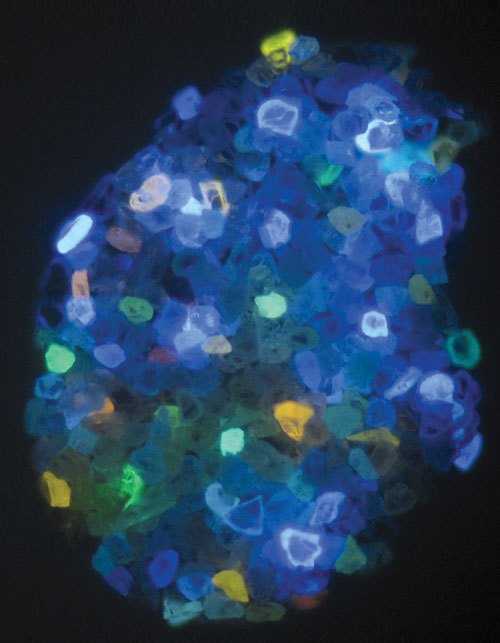
Natural diamond particles, each about 10 microns in diameter, fluoresce under exposure to UV light due to the presence of different tpes of defects. (Photograph by David Glenn and Huiliang Zhang, Harvard University.)
Atom-like systems can also be strongly coupled to other degrees of freedom, such as photons, phonons, or the spins of other electrons and nuclei in the crystal. The flexibility aids in the exploration of such systems. Moreover, the host crystal can be fabricated and integrated into a wide variety of devices large and small.
NV centers
The nitrogen–vacancy (NV) center in diamond is a prototypical example of an atom-like system. Formed by an impurity nitrogen atom sitting at a lattice site next to a missing carbon, or vacancy, an NV center can occur naturally or be created by nitrogen-ion implantation. The electrons that occupy the dangling bonds around the vacancy in each NV center are akin to electrons bound to the nucleus of an atom or ion insofar as they exhibit long-lived spin states and well-defined optical transitions. The electronic states lie deep within the wide indirect bandgap of diamond and are thereby energetically isolated from the extended valence-band states of the crystal.
Furthermore, diamond’s weak spin–orbit coupling, as well as its mostly spinless carbon-12 lattice, creates an ideal solid-state environment for spins. Despite the fact that the NV center is surrounded by nearest-neighbor atoms just angstroms away, its states are so well isolated from environmental perturbations that their spin coherence properties can be comparable to those of an ion trapped in ultrahigh vacuum.
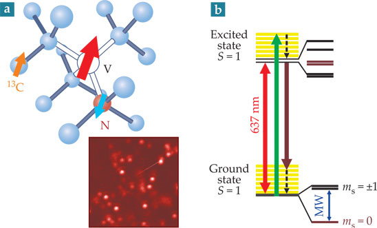
Much like an atom or ion, the NV center has an electronic structure that encompasses charge, orbital, and spin degrees of freedom. Beginning with spectroscopic work in the 1960s and notably spurred by the sustained efforts of Neil Manson’s group at Australian National University, a detailed understanding of the NV center’s structure has emerged. 1 The most interesting properties of the NV center lie in its negatively charged state. In that charge configuration, its ground state is an electronic spin triplet with long-lived Zeeman sublevels associated with spin projections ms = 0,+1,−1, as schematically shown in figure 1.

Figure 1. The structure of the nitrogen–vacancy (NV) center, a point defect made of a nitrogen atom substituted for carbon with an adjacent lattice vacancy. (a) In its negative charge configuration, the defect has a net electronic spin S =1 (red arrow) on the vacancy V, with nearby nuclear spins (blue and orange arrows) on nitrogen and carbon-13 impurities. In the confocal microscope image of diamond (inset), the fluorescence reveals individual NV centers. (b) The NV electronic state can be excited resonantly with 637-nm-wavelength light (red) or nonresonantly using shorter-wavelength light (green), after which the atom fluoresces at longer wavelengths (brown) following fast phonon relaxation. Black dashed arrows represent the relaxation through vibrational levels (yellow). Microwaves (MW) drive spin transitions between ms sublevels.
What makes the NV center stand out from other crystal defects is that the spin degree of freedom can be prepared and detected using its optical transitions. For example, the most common detection mechanism involves driving the NV center nonresonantly using visible laser pulses that excite an electronic transition to a higher-lying triplet state as well as some vibrations in the crystal lattice. Even with that nonselective excitation, the NV center fluoresces more brightly if its spin is in the state ms = 0. Furthermore, under continued excitation, the spin is pumped into the ms = 0 state within one microsecond, which conveniently enables both optical preparation and detection of the spin.
Optically detected spin resonance has been studied in ensembles of NV centers for several decades. But only recently, starting with the pioneering work of Jörg Wrachtrup, Fedor Jelezko, and coworkers, 2 has the method been applied to the spin states of individual NV centers. If the optical excitation and detection beams are focused on a single NV center, only that defect’s spin is prepared and detected. However, isolating single NV centers in an optical microscope and preserving their spin coherence requires a low density of NVs and other defects in the diamond lattice. Even a decade ago, only select natural diamonds offered sufficiently low defect densities. Fortunately, advances in chemical-vapor-deposition-based growth of diamond, led by Matthew Markham and Daniel Twitchen at Element Six, now allow researchers to work with custom-grown ultrapure material with defect densities below one part per billion. Moreover, NV centers with suitable properties can be realized both in bulk diamond and in nanodiamonds, and for high and low defect densities, which entail separations as close as nanometers or as far as many micrometers on average.
Thanks to the combination of confocal microscopy of high-purity samples and direct microwave manipulation of the NV spin states, monitoring the dynamics of a single spin is now routine. A typical experimental sequence begins with a pulse of light to optically pump the NV spin into the ms = 0 state. A microwave magnetic field—often applied as a high-intensity pulse using on-chip circuitry—in resonance with a spin transition can then precisely and rapidly manipulate the spin state. A final pulse of light induces fluorescence, whose brightness is proportional to the relative populations of the ms sublevels. The fluorescence signal thus provides a measure of the average spin polarization. The simplicity of that approach and its wide range of operating conditions have created a growing interest in using NV centers to probe fundamental physics, explore quantum information applications, and develop spin-based sensors.
At cryogenic temperatures, other optical techniques become possible. Whereas nonresonant excitation takes advantage of transitions involving both photons and phonons, resonant light near 637 nm, the so-called zero phonon line (ZPL), can directly drive the NV electronic transition alone, with no phonons required. Below around 20 K, an atomic-like fine structure is discernable within the ZPL. That structure corresponds to resolved transitions from the ground-state spin projections to specific excited-state sublevels that involve both spin and orbital degrees of freedom. Such spin-dependent resonant transitions exhibit many of the properties of atomic transitions.
From single spins to quantum registers
The coherence time of a spin determines how long quantum information can be stored in its states before leaking to the environment. It also sets the time over which the spin coherently evolves and can interact with applied fields, which is important for metrology. Protected by the small spin–orbit interaction in diamond, the NV spin only weakly couples to lattice phonons. The dominant spin-dephasing mechanism in high-purity samples comes instead from a dilute bath of nuclear spins associated with 13C atoms in the diamond lattice. Their effects can be mitigated by isotopic purification or by dynamical decoupling techniques, which eliminate the effect of the nuclear spins by continuously flipping the NV spin on a time scale much faster than any changes in the bath. 3 The effect is to extend the NV spin’s coherence time to several milliseconds at room temperature and to nearly one second at 77 K. Because microwave circuits fabricated in close proximity to the defect spin state can control it on nanosecond time scales, millions of operations can be performed before the spin decoheres. 3
Nearby nuclear spins, however, are not just a source of NV spin dephasing; in some cases they can also be individually addressed. That’s interesting and important because nuclear spins are among the most isolated quantum systems ever studied. Their coherence can persist for hours and their relaxation times can be measured in days. The difficulty lies in making that coherence useful: Nuclear spins interact so weakly with their surroundings and with each other that it is difficult to engineer mechanisms to control, couple, and detect them on realistic time scales.
Diamond’s NV center offers a solution, because its electronic spin can serve as an intermediary between optical controls and single nuclei. Specifically, the NV spin interacts most strongly with the closest nuclear spins, which leads to distinct hyperfine structures whose peaks depend on the location of the nearest 13C impurities. In the example in figure 2, the NV electron spin resonance frequency depends strongly on the joint state of the host 14N atom (with nuclear spin 1) and a nearby 13C atom (with nuclear spin ½). The visible hyperfine splittings show that nuclear spins within a few lattice sites of the center interact coherently with the NV spin far more rapidly than the bath of 13C nuclear spins dephases it.

Figure 2. Diamond defect as spin register. Optically detected magnetic resonance (a) shows the reduction in fluorescence of a nitrogen–vacancy (NV) center when its spin is driven by microwave (MW) pulses from ms = 0 to ms = −1. The transition occurs at different frequencies depending on the nuclear spin states of nearby carbon-13 (orange) and nitrogen-14 (blue). (b) The fluorescence time trace of a single NV center exhibits quantum jumps attributable to the 14N nuclear spin state of the defect. Applying a MW pulse acts like a controlled-NOT gate, flipping the electron spin in a way that’s conditional on the state of the nuclear spin. The fluorescence in the trace reveals the nuclear spin projection. (Adapted from ref.
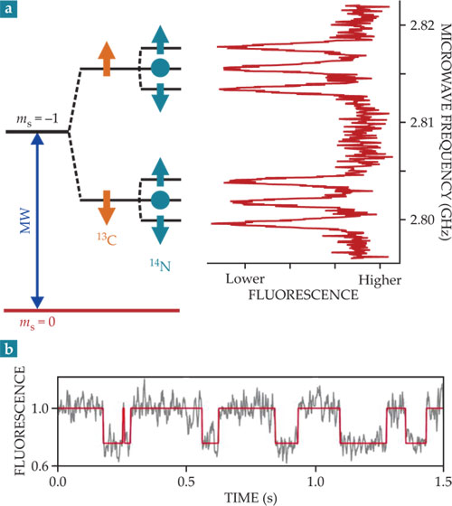
An NV center can thus be thought of as a hybrid spin register, in which the electronic spin serves as an access point to prepare and detect proximal nuclear spins. 4 Surprisingly, the detection fidelity for those nuclear spins can greatly exceed that of the NV electronic spin itself. The idea is to initialize the NV spin into the ms = 0 state and then flip the electron spin in a way that’s conditional on the 13C nuclear spin. That can be achieved by driving the hyperfine transition associated with a specific nuclear spin state, an operation equivalent to a controlled-NOT logic gate. The subsequent NV fluorescence level is thus correlated with the nuclear spin.
Moreover, unlike the electronic spin state, the nuclear spin orientation is not necessarily destroyed by optical excitation. That makes it possible to repeat the procedure many times to increase the signal-to-noise ratio. Hence, while the electron spin cannot always be fully detected before it relaxes, a weakly coupled nuclear spin—or, in principle, multiple nearby ones—can be detected repeatedly with high fidelity. One can even use the method to observe quantum jumps of the 14N and 13C nuclear spins using a single detected NV center (see figure 2b).
Such solid-state nuclear spins may find application in a long-lived quantum memory. Since the NV electronic spin can be polarized optically, researchers can average away spin fluctuations that could otherwise degrade the nuclear spin coherence lifetime. Through that mechanism, one can observe a 13C nuclear spin near a polarized NV center remain coherent for more than a second at room temperature; 5 even longer times are likely in cryogenic conditions. Recent experiments have established that electronic and nuclear spin states associated with a single NV center are a competitive platform for quantum information processing. For example, nuclear spins in the vicinity of NV centers have been used to violate Bell’s inequalities—the quintessential test of a system’s quantum nature—execute elementary quantum algorithms, and perform three-bit quantum error correction. 6
The number of spin qubits associated with a single atom-like defect is ultimately limited by the number of nuclear spins that can be spectrally resolved. Going beyond a few qubits will require coupling between atom-like systems. To that end, one can rely on the direct magnetic dipolar interactions between electronic spins. In the context of diamond, NV centers within a couple dozen nanometers of each other interact rapidly enough to entangle their electronic spin states before they decohere. Alternatively, one could use another, more mobile, quantum degree of freedom—for instance, photons or phonons—to mediate coherent interactions between NV centers.
Quantum interfaces
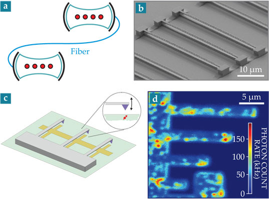
An optical photon is a natural “flying qubit,” capable of carrying quantum states encoded in its polarization, frequency, or timing over many kilometers. The capability can potentially link quantum registers to create a network akin to a quantum internet. 7 Practically, however, to collect, transmit, and deliver single photons with perfect efficiency is difficult, so a realistic scheme should be robust to photon loss.
One approach is to announce, or “herald,” the success of a protocol, often through the click of a photon counter, to ensure a high-fidelity interconnection even when photon collection efficiency is low. Put simply, distant atoms emit photons that are entangled with an atomic degree of freedom. The photons then meet at a central location and will, with some probability, swap their entanglement and thereby transfer it to the atoms. The photons trigger detectors if the swap was successful.
Originally developed in the context of atomic physics, 8 such heralded entanglement schemes can also be applied to atom-like systems. 9 In 2013 Ronald Hanson and his group at Delft University of Technology implemented such a scheme to realize entanglement between solid-state spins located on opposite sides of a laboratory. 10 Their experiments used electric fields to tune the optical transitions of two NV centers into resonance, and they used interference filters to extract just the ZPL emission, a step that ensured that the frequencies of the photons would be identical. As a result of the filtering, the photon collection efficiency was low; the scheme yielded one entangled pair in 10 million attempts. The approach has been used recently to achieve unconditional teleportation of a spin qubit. But the low success probability illustrates a central hurdle for experiments that use photons to mediate interactions between atom-like systems: creating an interface between the emitter and single photons that is both coherent and efficient.
Optical cavities may offer a way around the difficulty. Not only can they improve photon collection efficiencies, optical cavities can also enable coherent, deterministic interactions between single spins and single photons. The essence of the approach, known as cavity quantum electrodynamics, is to preferentially enhance the interaction between an emitter and a specific mode of the electromagnetic field by confining the mode for a long time in an optical resonator. If the interaction is strong enough, an excited atom will always emit a photon into the mode, and conversely, a ground-state atom will absorb a photon from the mode with near-perfect efficiency. (See Physics Today, September 2014, page 15 .)
Much of the groundbreaking work was begun in the 1990s by the groups of Jeff Kimble and Gerhard Rempe using ultracold atoms confined to Fabry–Perot cavities. More recently, nanophotonic systems have emerged as an attractive alternative thanks to their tight confinement of optical radiation and their replacement of real atoms, which need to be cooled and trapped, with solid-state emitters. Following work on semiconductor quantum dots in photonic-crystal cavities, researchers began coupling NV centers to a variety of optical resonators. Furthermore, advances in diamond fabrication pioneered by the groups of Marko Lončar, Ray Beausoleil, and Evelyn Hu have made it possible to create high-quality nanostructures in diamond itself, an integrated approach to efficient photon-mediated interactions between NV defects.
Other degrees of freedom besides photons can also be used to transport quantum states. Phonons, for instance, have long been used with great success in ion traps, where the collective motion of the ions represents the vibrational degrees of freedom. The same idea can be extended to solid-state devices by using a mechanical resonator to host long-lived phonon states and engineering the interactions between the resonator’s motion and a quantum system.
Figure 3 illustrates recent approaches taken to couple NV centers to mechanical resonators. For instance, a cantilever outfitted with a magnetic tip can interact with the spin state of a nearby NV center by inducing a Zeeman shift that varies with the cantilever position. 11 Alternatively, a mechanical resonator can be fashioned out of diamond itself, so that an NV center in the device will have an energy-level structure that shifts with motion-induced strain on the crystal. 12 For both mechanisms, achieving coherent spin–phonon interactions requires high-quality mechanical resonators and cryogenic temperatures. Nevertheless, if realized, the mechanical motion in such devices could be used to entangle NV centers. Furthermore, with modifications, the resonator could interact with different degrees of freedom—for example, a mirrored surface couples the resonator to light, and a metallic surface produces capacitive effects in electronic circuits—which makes for an appealing interface between disparate quantum devices.

Figure 3. Quantum interfaces for atom-like systems. A quantum network (a) can be depicted schematically as remote optical resonators containing atom-like qubits that interact via photons. (b) A series of photonic-crystal resonators fabricated from diamond provides one implementation of the scheme. (Adapted from M. J. Burek et al., Nano Lett. 12, 6084, 2012, doi:
Nanoscale sensing and imaging
Atom-like systems are attracting considerable interest as precision sensors. NV centers provide a unique combination of nT/√
To sense a magnetic field, one optically measures the Zeeman shift it induces in the NV center’s ground-state spin levels. Similarly, electric fields induce a linear Stark shift in the spin levels, 14 and temperature changes are discernable as changes in the zero-magnetic-field splitting between spin levels. 15 In addition, the diamond defect features several other appealing properties: Unlike fluorescent quantum dots, NV centers don’t blink, nor do they bleach under long exposure to laser light; they are geometrically adaptable, able to, for instance, sit on the tip of a force microscope cantilever, be implanted at high densities, or be dispersed via nanodiamonds in a host; and they are compatible with most materials, including metals, semiconductors, liquids, polymers, and biological tissues.
The optical stability of NV centers and their physical isolation within the diamond crystal make them ideally suited for super-resolution imaging detectors. In fact, NV centers hold the world record for far-field optical resolution—below 10 nm—and they have also been used for far-field nanoscale magnetic imaging. 16
By scanning a very strong magnetic field gradient over a single, shallow NV center, researchers can now perform three-dimensional magnetic resonance imaging (MRI) of single electron spins in a solid at 1-nm resolution; 17 the resolution in conventional MRI systems, by contrast, is limited to micrometers in solids and about one millimeter in biological tissue imaged in medical facilities. Ongoing efforts to use similar techniques to image dynamics of magnetic materials open prospects for mapping out states of complex matter. In addition, research groups have recently made nuclear magnetic resonance measurements of nanometer-sized volumes of proton spins. More specifically, they used a single, shallow NV center to detect a statistical polarization of only about 100 nuclear spins on the surface of a bulk diamond chip (see Physics Today, April 2013, page 12 ).
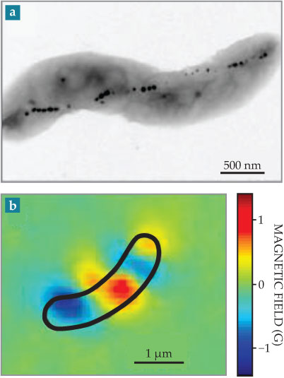
Some of the most exciting applications are in biology, where room-temperature functionality and inert chemistry are key (see Physics Today, August 2011, page 17 ). Exemplified in figure 4, magnetic imaging of living magnetotactic bacteria provides information about the distribution of magnetic moments among individual bacteria in the population. Local temperature changes can also be sensed, even within living human cells. Figure 5 illustrates how NV centers in nanodiamonds could be exploited to precisely monitor changes during targeted heating of a cell. The technique may even eventually mature into a way to selectively kill tumor cells.

Figure 5. Nanoscale thermometry senses the living and the dead. By placing a gold nanoparticle and nanodiamonds inside a living cell, one can simultaneously alter and monitor the cell’s condition. In this implementation, heat is applied to the gold (marked with an x in images) using laser light, and nitrogen–vacancy centers in the nanodiamond (marked with a circle) register changes in temperature as subtle shifts in spin frequency. Scanned confocal fluorescence images of an individual human cell, outlined in dashed lines, reveal its response to the applied heat. (a) With little laser-induced heating, the cell remains alive and experiences a modest half-kelvin rise above ambient temperature. (b) Greater heating kills the cell, its condition evident in the penetration of fluorescent stain through the cell membrane into the nucleus. The nanodiamond sensor recorded a rise of nearly 4 K. (Adapted from G. Kucsko et al., Nature 500, 54, 2013, doi:
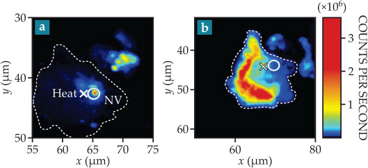

Figure 4. Magnetic imaging of living cells.(a) Magnetite nanocrystals appear as spots of high electron density in this transmission electron microscope image of a magnetotactic bacterium (MTB), whose organelles contain the magnetic crystals. The nanoparticles help the organism into alignment with Earth’s magnetic field. (b) Nitrogen–vacancy centers can image an MTB on the surface of a diamond chip. The bacterium’s magnetic field is imaged optically at 400-nm spatial resolution by monitoring the field-induced shift in the centers’ spin resonance frequency. The bacterium’s cell wall is outlined in black. (Adapted from D. Le Sage et al., Nature 496, 486, 2013, doi:
Outlook
Much work remains in order to exploit the full potential of atom-like systems. For example, building a room-temperature quantum processor whose logic gates are based on coupled NV centers would require nanometer-level control over defect placement or techniques that control the quantum dynamics of disordered systems. To realize the promise of diamond nanophotonics, mitigating fluctuations in the NV center’s fluorescence frequency caused by undesired impurities in the crystal will be essential. Progress on NV nanoscale sensing and nanoscopic MRI will similarly require exquisite control over the diamond surface and the attachment of target molecules to it.
In addition to NV centers, many other atom-like defects—in diamond and other wide-bandgap materials—are active research topics. For example, silicon-vacancy centers, which have been explored by Christoph Becher, Mete Atatüre, and coworkers, efficiently produce coherent optical photons with excellent spectral stability and very low probability of phonon-assisted emission. Their properties make them an intriguing alternative to NV centers for quantum optics and networking applications. In their work on phosphorous dopants in silicon, Andrea Morello and John Morton and coworkers have achieved excellent control of both electronic spin and nuclear spin qubits. And David Awschalom and coworkers have identified defects in silicon carbide that can be manipulated in a manner similar to NV centers (see Physics Today, January 2012, page 10 ).
Research on atom-like systems is likely to help answer major scientific and technological questions. For instance, studies of coherently coupled NV centers may reveal fundamental insights on equilibration, coherence, and entanglement in many-body systems. In the domain of optics, atom-like defects may become the building blocks of nonlinear optical devices that operate at the single-photon level. And experiments on quantum networks could lead to laboratory realizations of repeater stations for long-distance quantum communication.
In the life sciences, atom-like sensors may someday be used to directly image the structure of complex individual molecules, a long-standing goal in the MRI community. In vivo measurements of electromagnetic fields and temperature may become tools for temperature-induced control of gene expression and tumor metabolism. Finally, atom-like systems could potentially be employed to image, noninvasively and in real time, firing neurons in the brain. All these possibilities have created an exceedingly rich, exciting, and interdisciplinary research frontier.
We thank NSF, CUA, DARPA, NIST, AFOSR, ARO, CFI, NSERC, FRQNT, and Moore Foundation for supporting this work.
References
1. M. W. Doherty et al., Phys. Rep. 528, 1 (2013). https://doi.org/10.1016/j.physrep.2013.02.001
2. A. Gruber et al., Science 276, 2012 (1997); https://doi.org/10.1126/science.276.5321.2012
F. Jelezko et al., Phys. Rev. Lett. 92, 076401 (2004). https://doi.org/10.1103/PhysRevLett.92.0764013. G. Balasubramanian et al., Nat. Mater. 8, 383 (2009); https://doi.org/10.1038/nmat2420
G. D. Fuchs et al., Science 326, 1520 (2009). https://doi.org/10.1126/science.11811934. M. V. G. Dutt et al., Science 316, 1312 (2007); https://doi.org/10.1126/science.1139831
P. Neumann et al., Science 329, 542 (2010). https://doi.org/10.1126/science.11890755. P. Maurer et al., Science 336, 1283 (2012). https://doi.org/10.1126/science.1220513
6. G. Waldherr et al., Nature 506, 204 (2014); https://doi.org/10.1038/nature12919
T. H. Taminiau et al., Nat. Nanotechnol. 9, 171 (2014). https://doi.org/10.1038/nnano.2014.27. H. J. Kimble, Nature 453, 1023 (2008). https://doi.org/10.1038/nature07127
8. L.-M. Duan, C. Monroe, Rev. Mod. Phys. 82, 1209 (2010). https://doi.org/10.1103/RevModPhys.82.1209
9. E. Togan et al., Nature 466, 730 (2010). https://doi.org/10.1038/nature09256
10. H. Bernien et al., Nature 497, 86 (2013). https://doi.org/10.1038/nature12016
11. S. Kolkowitz et al., Science 335, 1603 (2012). https://doi.org/10.1126/science.1216821
12. P. Ovartchaiyapong et al., Nat. Commun. 5, 4429 (2014).
13. See, for example, J. M. Taylor et al., Nat. Phys. 4, 810 (2008). https://doi.org/10.1038/nphys1075
14. F. Dolde et al., Nat. Phys. 7, 459 (2011). https://doi.org/10.1038/nphys1969
15. See, for example, V. Acosta et al., Phys. Rev. Lett. 104, 070801 (2010); https://doi.org/10.1103/PhysRevLett.104.070801
P. Neumann et al., Nano Lett. 13, 2738 (2013). https://doi.org/10.1021/nl401216y16. E. Rittweger et al., Nat. Photon. 3, 144 (2009); https://doi.org/10.1038/nphoton.2009.2
P. C. Maurer et al., Nat. Phys. 6, 912 (2010). https://doi.org/10.1038/nphys177417. M. S. Grinolds et al., Nat. Nanotechnol. 9, 279 (2014). https://doi.org/10.1038/nnano.2014.30
More about the authors
Lilian Childress is an assistant professor of physics at McGill University in Montreal; Ronald Walsworth is a senior lecturer on physics at Harvard University and a senior physicist at the Smithsonian Astrophysical Observatory in Cambridge, Massachusetts; and Mikhail Lukin is a professor of physics at Harvard University in Cambridge, Massachusetts.


