Flexible circuits
DOI: 10.1063/1.2930748
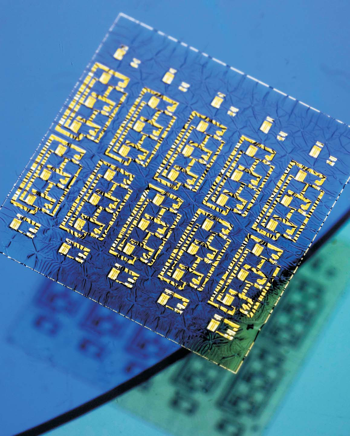
Recent work by John Rogers and colleagues at the University of Illinois at Urbana-Champaign has successfully combined the high performance of silicon-based electronics with the flexibility and stretchability of elastomeric materials. The resulting devices can be twisted and stretched, with strains as high as 10%, and even folded over the edge of a microscope cover slip—all with essentially no effect on the circuit behavior.
Rogers and company use a transfer-printing technique to deposit CMOS circuits onto a flexible polyimide layer 1.2 microns thick. The resulting system is extremely bendable yet functional for two reasons: The layered structure is thin, and the neutral mechanical plane—the plane in which the strains are zero when the structure is bent—lies within the electronics. The system can be compressed and stretched by bonding it to a prestrained polydimethylsiloxane substrate. When the PDMS layer is allowed to relax, the layers buckle and form a complex wavy pattern like that seen in this sheet, which features two rows of ring oscillators above a row of inverters. The linewidths in these circuits are about 100 microns; the smallest features, 10 microns. (D.-H. Kim et al., Science Express, http://dx.doi.org/10.1126/science.1154367 ; image courtesy of John Rogers.)
To submit candidate images for Back Scatter, visit http://www.physicstoday.org/backscatter.html .

image courtesy of John Rogers


