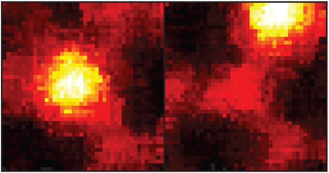
Walking a silicon atom through a graphene landscape
DOI: 10.1063/PT.3.2503
The electron beam in a transmission electron microscope (TEM) can displace atoms in a sample and sometimes cause what’s called knock-on damage.Researchers at the University of Vienna, together with UK teams at the Daresbury SuperSTEM Laboratory and the University of Manchester and a team from Nion Co in the US, have now used those displacements to manipulate a sample one atom at a time. During TEM scans of silicon-doped graphene, they found that the electron beam can cause a Si atom to hop from one lattice site to a neighboring one about 0.14 nm away. The two TEM images here, taken 0.5 seconds apart, show a Si atom (bright spot) before and after such a hop. The hop itself happens on a time scale too fast to see with a TEM, so the researchers turned to molecular dynamics simulations, which showed that the electron beam actually knocks out a carbon atom. But instead of escaping, the ejected C atom curves back toward the neighboring Si atom because of their mutually attractive interaction. At the same time, the Si atom relaxes toward the newly created vacancy. When all is said and done, the two atoms have swapped positions. Since the hopping is induced by displacing a C atom rather than directly affecting the Si atom, the researchers suggest that a narrow electron beam could direct the movement of a Si atom to any desired site. (T. Susi et al., Phys. Rev. Lett., in press


