Silicon carbide defects hold promise for device-friendly qubits
DOI: 10.1063/PT.3.1410
The central element of any quantum computation scheme is the qubit, a two-state system analogous to the spin-1⁄2 electron. In the course of a computation, the qubit experiences various changes in its state; once the calculation is completed, one needs to determine whether the qubit is “up” or “down.” Unfortunately, the qubit also has to interact with its thermal environment, which can destroy, or decohere, its quantum state. Any useful qubit, then, must be able to resist decoherence for as long as it takes to do a worthwhile sequence of quantum manipulations.
Several systems could conceivably meet that criterion, from Josephson junctions (see PHYSICS TODAY, July 2009, page 14 ) to quantum dots (see PHYSICS TODAY, March 2011, page 19 ). Of the solid-state candidates, however, nearly all must be chilled to cryogenic temperatures to obtain suitable coherence times
One exception is an atomic-scale diamond impurity known as an NV center, in which a nitrogen atom and a vacancy substitute for two neighboring carbon atoms. The electron spin state of an NV center can remain coherent for more than a millisecond at room temperature. What’s more, the spin state can be manipulated with microwaves and conveniently read out via optical fluorescence.
The diamond NV center, then, is in many ways the ideal qubit. Nonetheless, it has yet to liberate quantum computing schemes from the confines of the cryostat. The reason is foremost a practical one: Quantum computing requires that qubits interface with each other through logic gates and with a host of peripheral components. Diamond is neither cheaply nor easily processed into such sophisticated devices.
But what makes diamond so special? That question was posed last year by researchers at the University of California, Santa Barbara, led by David Awschalom and Chris Van de Walle. 1 Among diamond’s virtues, they noted, is its wide bandgap relative to the splitting between the ground and excited electronic states of an NV center. That means a diamond-embedded NV center can be fluorescently probed without losing electrons to the bulk. Furthermore, diamond’s weak spin–orbit coupling and its predominantly spin-0 carbon nuclei help to minimize the influence of the environment on the qubit state.
Recognizing that those traits aren’t unique to diamond, the UCSB group set out to find other materials that might host long-lived qubits. They’ve now found promising candidates lurking inside ordinary wafers of silicon carbide, 2 a material that’s already widely used for high-power electronics. Although it’s not clear that any of the newfound qubits are NV centers, they are all atomic-scale defects and two have long-lived spin states at room temperature.
Seeking imperfection
Silicon carbide is a natural stand-in for diamond; Si sits just below C on the periodic table and the two materials have similar electronic properties and structure. The team’s quantitative calculations suggested, however, that NV centers in the two materials would differ in one key regard: The energy spacings between the ground and excited states of SiC’s NV centers were predicted to be about half those in diamond, so whereas the diamond defects fluoresce in the visible, the SiC defects would fluoresce in the near-IR.
Indeed, lab experiments revealed six sharp emission lines, ranging in wavelength from roughly 1035 nm to 1135 nm, in the fluorescence spectra of chilled SiC samples. Four of the peaks, known as PL1–PL4, turned out to originate not from NV centers but from divacancies—missing pairs of neighboring C and Si atoms. The other two, PL5 and PL6, had never before been detected and originate from as-yet unidentified defects.
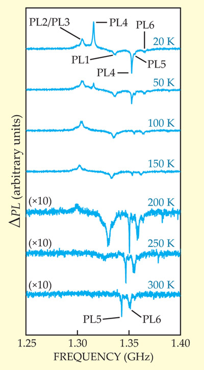
How could a divacancy—a little bit of nothing—be regarded as a qubit? In fact, the qubit comprises the collective of atoms in the vicinity of the vacancy. Electrons that would have been bound to Si or C in the unblemished lattice are left unpaired and localized at the divacancy. Like diamond’s NV centers, those electron spin states, as well as those of SiC’s two unidentified defects, can be read via optical fluorescence. As shown in figure 1, irradiation of SiC with microwaves elicits a sharp increase or decrease in photoluminescence intensity at each defect’s spin-resonance frequency. Although the spin-resonance signals weaken with increasing temperature, the peaks corresponding to PL5 and PL6 survive to 300 K, so those defect spin states are readable at room temperature.

Figure 1. Irradiation of a silicon carbide sample with microwaves yields a sharp change in photoluminescence intensity P at the spin-resonance frequencies of six photoluminescent defects, PL1–PL6. (A spin–spin splitting in the defect corresponding to PL4 results in that defect showing two spin resonance frequencies.) Although the spin-resonance signals weaken with increasing temperature, PL5 and PL6 persist to room temperature. (Adapted from ref.
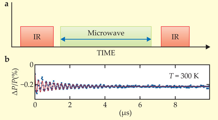
Also like diamond’s NV centers, the orientations of the SiC defect spins could be controlled with techniques borrowed from nuclear magnetic resonance. Figure 2 illustrates one example, in which the researchers polarized an ensemble of defect spins with an IR pulse, rotated the ensemble with a microwave pulse, and detected the oscillations in the spin orientation via fluorescent probing. Applying a more sophisticated pulse sequence, the researchers showed they could coherently control spins for over 100 µs in chilled samples and for over 40 µs at room temperature. Provided SiC’s defect spins can be flipped as swiftly as those of diamond’s NV centers—that is, about once per nanosecond—a SiC qubit could conceivably survive thousands of quantum operations at room temperature.

Figure 2. Coherent control. Applied to a sample of silicon carbide, the pulse sequence shown in (a)—an IR pulse followed by a microwave pulse of length τ followed by a second IR pulse—polarizes defect spins, rotates them, and then elicits a burst of photoluminescence that hints at their final orientation. Repeating the pulse sequence for various τ yields the data points (blue symbols) and fit (red curve) shown in (b). The oscillations in photoluminescence intensity P suggest coherent rotations of the ensemble of electron spins. The data show the room-temperature response of one of SiC’s as-yet unidentified defect structures. (Adapted from ref.
All of the team’s experiments were performed on defect ensembles; the millimeter-sized samples of SiC contain roughly 100 defects per cubic micron. Key to proving the defects’ utility as qubits will be demonstrating that each one can be controlled individually. One challenge, says Awschalom, is detecting single photon emissions. That task is relatively straightforward in the visible but much more difficult in the IR. The researchers are now collaborating on that effort with NIST in Boulder, Colorado. Also key to realizing quantum devices will be demonstrating entanglement between multiple qubits and integrating them with photonic, electronic, and micromagnetic structures.
That the SiC defects emit in the near-IR and in the vicinity of fiber-optic bandwidths could ultimately prove a significant advantage. Says Awschalom, “It would mean that you could do quantum manipulation in the same material that’s already being used for electronics, at telecommunications frequencies—and all at room temperature.”
Jörg Wrachtrup (University of Stuttgart, Germany), who pioneered the manipulation of single-defect spin states in diamond, sees potential applications for SiC defects beyond quantum computing. He cites the defects’ promise as ultrasensitive magnetometers. (See PHYSICS TODAY, August 2011, page 17 .) Says Wrachtrup, “I could envision using tiny silicon carbide crystals to do micro- or nanoscale magnetic resonance imaging on cells and other biological systems. It really could open up a whole new world of scientific applications.”
References
1. J. R. Weber et al., Proc. Natl. Acad. Sci. USA 107, 8513 (2010). https://doi.org/10.1073/pnas.1003052107
2. W. F. Koehl et al., Nature 479, 84 (2011).https://doi.org/10.1038/nature10562


