Semiconductor industry switches to hafnium-based transistors
DOI: 10.1063/1.2883902
Some day semiconductor chip components may cease to shrink; that day is not now.
At the December 2007 International Electron Devices Meeting, Intel Corp presented a paper, written by 50 of its scientists and engineers, that unveiled details of the company’s 45-nm technology. The new technology features more efficient materials that replace, for the first time in almost 40 years, polycrystalline silicon gate electrodes and silicon oxide–based insulators—core components of the transistor, the on/off switch of an integrated circuit.
The move was a response to a line in the sand drawn by fundamental physical limitations. As key circuit features shrank to single-digit nanometer dimensions, quantum tunneling of charge carriers through thinning silicon-based insulators, also called gate dielectrics, threatened the continuation of Moore’s law—the doubling of transistor density approximately every two years. The semiconductor industry could no longer ignore the power loss and excessive heating that resulted from the leakage currents and was forced to seek an alternative material.
Several semiconductor companies—including Texas Instruments Inc and IBM and its partners—have committed to producing chips that use high-dielectric-constant hafnium oxide–based insulators and metal-gate electrodes, called “high-k metal-gate” technology (k represents the Greek letter kappa, which represents the dielectric constant), by 2008 or 2009. Intel’s 45-nm product, launched last November, uses the new hafnium-based technology.
Industry road-map target
The hunt for high-k dielectrics began when the industry could no longer shrink the gate dielectric beyond the tunneling limit, says Thomas Theis, director of physical sciences at the IBM Thomas J. Watson Research Center. Since 1992 the semiconductor industry has been urged by what is now the International Technology Roadmap for Semiconductors to shrink various features on an integrated circuit in an effort to sustain Moore’s law. Each successive shrinking or scaling is known as a technology generation or node. The road map, normally updated yearly and commissioned by industry associations from the five leading chip-manufacturing regions in the world—Japan, South Korea, Europe, Taiwan, and the US—gives a 15-year outlook of the R&D needs of the semiconductor industry.
In the mid-1990s, however, the industry became concerned that as the transistor components shrank, too many electrons would tunnel through silicon dioxide layers. High capacitance in a transistor drives performance and is proportional to the dielectric constant but inversely proportional to the insulator’s thickness. Near the turn of the 21st century, the thinning of the silicon dioxide insulator, which has a modest dielectric constant of about 3.9, started to become significant below thicknesses of 2 nm. As the thickness approached 1 nm, the leakage current approached 100 A/cm2—an unacceptable rate that produces power drain and overheating especially for low-power devices such as cell phones and laptops.
Laying the groundwork
Attention to the need for high-k gate insulators was widely disseminated after the 1997 road map, says Carlton Osburn, a researcher at North Carolina State University. That report initiated extensive precompetitive and collaborative research to find the best high-k materials and the processes for incorporating them. In the US in 1997, SEMATECH, a nonprofit industry research consortium, and the Semiconductor Research Corp (SRC), an industry consortium sponsoring research at more than 100 universities worldwide, jointly funded a research center in 1997 based at NCSU to tackle the high-k challenge. Researchers from 14 universities affiliated with the center evaluated hundreds of combinations of gate dielectrics and gate electrode materials, says Osburn, who directed the NCSU center. He added that the center played a pivotal role in identifying the hafnium oxide family of materials as the best candidates for the gate insulator.
In Europe, the Belgian Interuniversity Microelectronics Center, or IMEC, whose members include academic and industrial institutions around the world, conducted similar research. “University collaborations are used [by industry] to lay the groundwork and build the knowledge base upon which they can implement what they plan to do,” says Michael Polcari, president and CEO of SEMATECH. In addition to the material breakthroughs, Raj Jammy, a technical director at SEMATECH, also credits atomic layer deposition as critical to high-k metal-gate integration.
But even before the precompetitive work, high-k research activity was being done at companies like Bell Labs, IBM, and Intel “in secret,” says Steven Hillenius, vice president of research operations at SRC, “but no one [company] had it all.” Intel’s internal research began around 1996 and continued until about 2003, says Michael Mayberry, who was involved in Intel’s early high-k explorations and is vice president of the company’s components research group. “High-k metal-gate transistors are just the latest example of the types of breakthroughs that our industry needs to keep Moore’s law going,” says Mark Bohr, a senior fellow with Intel’s logic technology development group. “And [to] anyone who was suggesting that Moore’s law has run out of steam, I would say this is evidence to the contrary.”
For the moment, device manufacturers are keeping the actual recipes for their high-k and metal-gate materials under wraps. Osburn says that the gate insulator is likely a derivative of hafnium oxide with dielectric constant six to eight times that of SiO2. Hafnium oxide “is refractory enough to withstand the demands of high-temperature silicon processing,” says Supratik Guha, a senior manager at IBM and a member of its original high-k research group. For the metal-gate electrode, many metal alloy solutions have been explored, including tantalum carbide, lanthanum, and aluminum-based materials.
Robert Doering, a senior fellow and technology strategist for Texas Instruments, says that high-k technology will not meet the requirements for high-volume, low-power devices until the 32-nm generation. High-performance device customers, however, are still assessing their need for high-k at 45 nm, he adds. The Japanese chip maker NEC Corp has put high-k technology in application-specific integrated circuits at the 55-nm generation. An IBM-led alliance, whose members have not yet been disclosed, plans to introduce high-k metal-gate technology for the 32-nm generation.
The gate debate
“High-k was never thought to be commercializable because it had defects that trapped charge and caused the parameters of the transistor to shift over time,” says John Suehle, who leads semiconductor device reliability and characterization studies at NIST in Gaithersburg, Maryland. Choosing the appropriate gate-electrode material presented additional constraints. “The whole history of searching for both high-k gate dielectrics and metal gates is really very long,” says Doering, adding that aluminum metal gates were being used in some of the early metal-oxide semiconductor transistors in the 1960s.
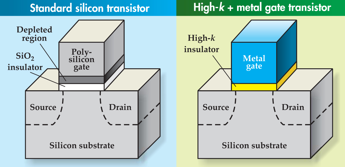
Polysilicon, though not as conductive as most metals, became the industry choice for the gate electrode because it was easier to fabricate and integrate, it interfaced better with SiO2, and it could be easily doped for optimum threshold voltage—the voltage at which electrons or holes begin to flow from the source to the drain. Yet the polysilicon gate electrode brought about depletion of carriers at the electrode–insulator interface of thin insulators, the so-called poly-depletion effect. Consequently, the semiconductor industry is returning to metal-gate electrodes, but with new metals, to interface with the hafnium materials (see the figure on page 25).

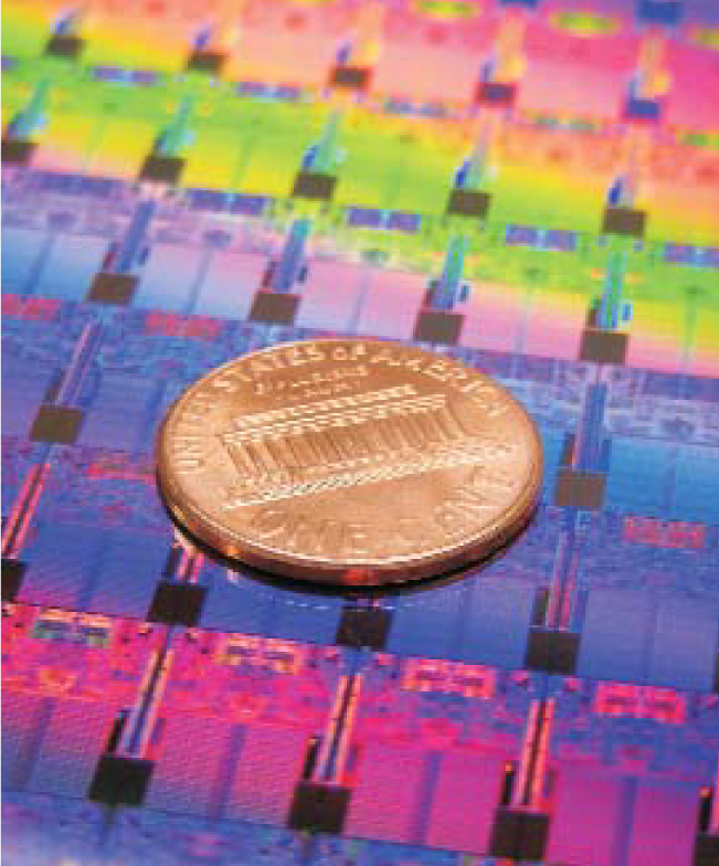
Intel’s newest 45-nm microprocessors are now in production and incorporate, for the first time, transistors using hafnium-based insulators and metal gates.
(Courtesy of Intel Corp.)
Since conventional transistor processing includes a high-temperature annealing step that could lead to diffusion of the metal into the gate dielectric material, Intel chose to go with a “high-k-first, gate-last process,” says Intel’s Bohr, referring to the order of deposition. The company is also opting for two different metal-gate materials to provide better control of threshold voltages. The nontraditional gate-last is viewed by Intel’s competitors as potentially more expensive than the current gate-first process, since it involves adding and removing a sacrificial layer between the dielectric and the metal gate. Bohr says that the cost increase to produce the 45-nm technology high-k wafers is only about 3%, with the performance boost and power reduction providing a good return on investment.
IBM is going with a gate-first process and will be using only one type of electrode material, whereas Texas Instruments plans to go with gate-first but has also developed a gate-last process, says Doering. “It would be difficult to know which process is best until they all ramp up to volume manufacturing,” says Hillenius, adding that gate-first and gate-last may end up being equivalent processes.
As scaling continues, Doering says, the industry will continue to search for newer compatible materials with even higher dielectric constants than the hafnium oxides. Meanwhile, university and industry researchers are simultaneously looking for solutions beyond silicon as industry forecasters predict the inevitable demise of Moore’s law.
“Stephen Hawking came through Silicon Valley a few years ago,” recalls Gordon Moore, Intel’s cofounder and author of Moore’s law. According to Moore, someone at a presentation given by Hawking asked the theoretical physicist what the limitations to the law would be. Hawking replied, “the speed of light and the atomic nature of matter.”
“That turns out to be pretty much the case,” Moore says.

The new standard for smaller transistors will be high-dielectric-constant hafnium-based materials and metal-gate electrodes that will replace the silicon oxide–based insulator and the polysilicon gate. In the figure, k represents the dielectric constant.

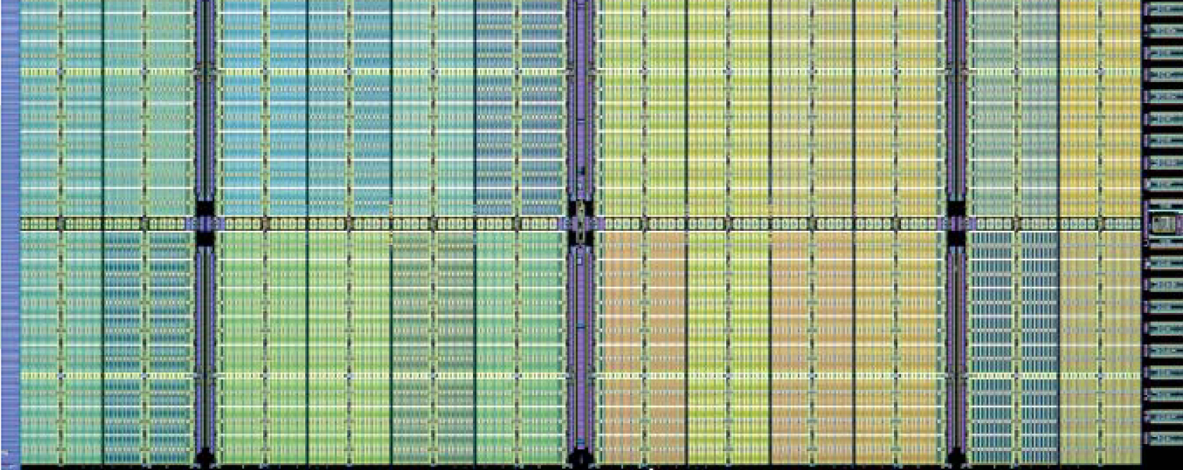
IBM’s 32-nm technology chips featuring hafnium-based insulators and metal-gate electrodes are promised for delivery to its alliance members and their clients by 2009.
(Courtesy of IBM.)


