Nobel physics prize honors achievements in graphene
DOI: 10.1063/1.3528996
In his 1996 Nobel lecture on the discovery of fullerenes, Richard Smalley made a prescient remark: “We are still in the process of discovering all the other consequences of the genius that is wired into carbon atoms.” This year the Royal Swedish Academy of Sciences has recognized a new chapter in carbon research by awarding the Nobel Prize in Physics to a pair of Russian-born scientists—Andre Geim, director of the Centre for Mesoscience and Nanotechnology at the University of Manchester in the UK, and his former PhD student and postdoc Konstantin Novoselov, now a professor also at the University of Manchester—“for groundbreaking experiments regarding the two-dimensional material graphene.” The two colleagues will split the prize of about $1.4 million.
The pair’s first experiments were published six years ago. Four years earlier, while Geim was at the Radboud University Nijmegen in the Netherlands and Novoselov was a graduate student there, Geim and Bristol University’s Michael Berry were awarded a satirical Ig Nobel prize for using a 20-tesla magnet to levitate a frog by means of diamagnetism (see Physics Today, September 1998, page 36 ). Geim stands alone as the first individual to win both prizes, and Berry, coincidentally, is linked to one of graphene’s central features—the Berry’s phase, which is at the heart of the material’s anomalous quantum Hall effect.
What’s old is new
This year marks the 25th birthday of Smalley’s buckyballs and nearly the 20th anniversary of Sumio Iijima’s report of finding carbon nanotubes, the 1D allotrope of carbon, in the soot from an arc discharge used to make fullerene clusters. Graphene, a one-atom-thick sheet of carbon arranged in a honey-comb lattice, can be thought of as an unwrapped buckyball or an unrolled nanotube, though it isn’t normally synthesized from either structure.
Whereas buckyballs and nanotubes were strikingly new objects—at least experimentally—when they were first observed in the laboratory, graphene has been an object of interest for more than half a century. It’s been studied theoretically since 1947, when Philip Wallace first mapped out its band structure, 1 and experimentally since 1962, when organic chemist Hanns-Peter Boehm chemically synthesized graphene from graphite oxide in solution and observed the atomically thin fragments by transmission electron microscopy. 2
In the 1970s materials scientists began growing graphene and ultrathin graphite films on surfaces such as nickel and silicon carbide. That approach has now matured, but at the time the carbon films were thought to have little practical value and interest in them remained minor and purely academic. Indeed, it wasn’t until 1994 that Boehm and colleagues officially coined the word “graphene” as acceptable parlance in the literature.
In the 1990s, while carbon nanotubes were gaining rock-star status as a promising electronic material, a handful of researchers began pursuing different tacks to isolate graphene. Rodney Ruoff (now at the University of Texas at Austin) pioneered one approach. In 1999 he patterned a graphite surface into macroscopic pillars that, when rubbed against a Si wafer, would create thin multilayer flakes that spread out like a deck of cards.
Inspired by that approach, three years later Columbia University’s Philip Kim engineered a sophisticated “nanopencil” by replacing the tip of an atomic force microscope with a tiny chunk of graphite. He also found flakes of graphite, some as thin as 10 monolayers, or about 4 nm. But a single layer remained elusive. At the same time, Walt de Heer, of the Georgia Institute of Technology, was also building on an earlier method, controllably evaporating away Si from SiC to leave behind ultrathin graphite; his work aimed squarely at the development of graphene electronics.
The summer after Kim presented his work at the 2004 March Meeting of the American Physical Society, he began hearing rumors that Geim’s Manchester group was also working on the problem. “In September, when I read a preprint of Andre’s article and realized he had isolated a single graphene layer, I was deeply shocked and felt scooped, of course. Then, after a second, closer read, I realized the technique involved Scotch tape—another big shock!”
Geim, Novoselov, and their collaborators had developed an exceedingly simple, cheap, and quick method for making high-quality, device-ready graphene: using tape to repeatedly peel away weakly bound layers from a graphite crystal and then gently rubbing those layers onto an oxidized silicon surface. Most crucially, they described how to locate the rare graphene flakes in the haystack of thicker, multilayer flakes using an optical microscope. On a SiO2 surface of just the right thickness, graphene reveals itself through interference fringes. 3 (See figure 1 and the article by Geim and Allan MacDonald in Physics Today, August 2007, page 35 .)

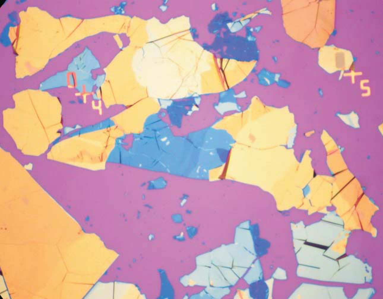
Figure 1. Different colors in this 300-µm-wide optical micrograph reveal graphite flakes with differing thicknesses peeled with Scotch tape from bulk graphite and then rubbed onto an oxidized silicon wafer. Individual atomic planes of graphene are hidden in the debris but can still be found by zooming in and searching for flakes with the weakest contrast. Force microscopy is then later used to measure the thicknesses.
(Courtesy of Peter Blake.)
The method—“essentially creating in parallel and optically screening millions of nanopencils,” Kim says—was efficient and its description was detailed enough to follow. Its utter simplicity, comments Boston University’s Antonio Castro Neto, made graphene “democratic” and spawned a cottage industry of peeling and rubbing. Anyone armed with tape and a chunk of graphite could make samples.
To date, more than 2200 articles with “graphene” in the title have appeared in Applied Physics Letters, Nature, Science, and the Physical Review family of journals. All but 28 of them have come out since 2005.
Behind the myth
The Manchester project began as a longshot attempt to devise a 2D metallic transistor. The trick for making samples emerged from what Geim calls “hit and run” experiments. “We just try all kinds of crazy things that probably won’t pan out,” says Novoselov. “Andre had done frog levitation as one of those experiments, and we did ‘;gecko tape’ together. The Scotch-tape idea—a totally routine technique—actually came from a microscopy postdoc [Oleg Shklyarevskii, now at Radboud University Nijmegen] in the lab.”
The team got lucky in another respect as well. The SiO2 sample the pair used as a substrate for the rubbed graphite flakes was 300 nm thick. A difference in thickness of just a few percent, the researchers later realized, would have made graphene completely invisible. 4 “That saved us months,” Novoselov recalls. Within a week the team had painted electrical leads and fashioned a working FET out of a few graphite layers, a step that provided an important proof of concept.
But getting down to single-layer graphene took about a year. “It looks absolutely trivial now that we understand exactly what to look for, but at the start it wasn’t at all,” he says. Geim adds, “The common impression of graphene emerging as if from thin air is a nice myth.”
A portrait of two dimensions
In 2005 Geim’s Manchester group and Kim’s Columbia group published back-to-back accounts of graphene’s 2D electron-gas physics. 5, 6 The researchers’ independent observations of the material’s quantum Hall effect proved it to be a remarkable conductor with exotic properties—in particular, that its mobile electrons behave as if they were massless, relativistic fermions (see Physics Today, January 2006, page 21 ).
In ordinary semiconductors, an electron can be modeled as a particle that obeys Newton’s laws of motion, provided it is ascribed an effective mass that accounts for the electron’s interactions with the crystal lattice. The electron’s energy thus depends quadratically on its momentum, and its quantum mechanical behavior can be described by the Schrödinger equation.
Thanks to the symmetry of the honeycomb lattice, graphene’s electrons behave differently. They experience a linear dependence of energy on momentum and therefore have the same quantum dynamics as elementary particles described by the Dirac equation. The material’s valence and conduction bands meet and cross at the so-called Dirac point, which looks like the tip of two inverted cones in momentum space. Electrons fly through the material as if they were photons or neutrinos but with an energy-independent velocity some 300 times smaller than the speed of light.
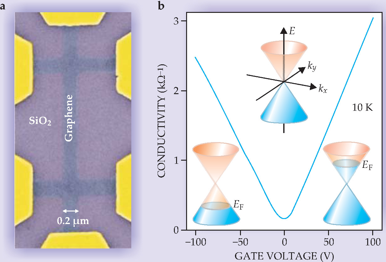
Geim’s and Kim’s groups mapped out the unusual dispersion curve by measuring the response of graphene’s electrons to electric and magnetic fields. One of their first experiments was to measure the conductivity by systematically tuning the position of the Fermi level, the highest energy level occupied by electrons, as shown in figure 2. Electrons and holes conduct continually through the material, even at the point between bands where no charge carriers should exist.

Figure 2. The ambipolar electric field effect in graphene. (a) By attaching a gate electrode to the back of a silicon dioxide substrate on which a graphene crystal sits, the University of Manchester group formed a metallic FET; the gold pads provide electrical access to the graphene. (b) The carrier density in graphene can be adjusted by simply tuning the gate voltage. The conductivity is measured by sweeping the Fermi level E F across a range of low energies, where graphene’s energy dispersion as a function of wave vector k is linear.
(Adapted from
The connection to relativistic physics is even deeper. Dirac’s theory explains why electrons have spin. But when applied to graphene, the theory endows the electrons with a so-called pseudospin, again due to peculiar symmetries of the honeycomb lattice. Interesting physics shows up in graphene’s quantum Hall effect. When an electron completes a full cyclotron orbit in a magnetic field, the rotation of the pseudospin introduces a 180° phase shift in the electron’s wavefunction. That modification (the Berry’s phase) changes the pattern of allowed quantized energies.
The pseudospin has other consequences: It protects graphene electrons against backscattering off defects and impurities. As the University of Maryland’s Michael Fuhrer explains, “For an electron to backscatter as it conducts, it would have to reverse not just its momentum but also its pseudospin, which is forbidden.” The effect is to enhance the conduction, and it explains why charge carriers in graphene tend not to localize.
In graphene, experimentalists have a material whose dynamics they can directly access with various scanning probes at room temperature and beyond—up to its melting point, in principle—because the electrons are forced to live in a strictly 2D plane. In 2007 Geim, Novoselov, and their colleagues observed graphene’s quantum Hall effect at room temperature, a measurement that in traditional 2D systems requires ultralow temperatures, often below the 4-K boiling point of liquid helium.
A simple tight-binding, noninteracting-electron model describes graphene remarkably well. 1 But last year researchers found intriguing results suggesting that the material also exhibits a fractional quantum Hall effect, evidence that electrons can, in fact, strongly interact to form a collective state with fractional charge. The measurements raise interesting questions about what exactly happens at the Dirac point when a strong magnetic field is applied—whether graphene remains conducting or ever makes a transition to an insulating state (see Physics Today, January 2010, page 11 ).
Graphene’s simplicity for theorists and experimentalists alike makes it a valuable testbed for concepts relevant to more complicated or fragile materials, such as topological insulators or d-wave superconductors.
New electronics
Most materials cannot exist as 2D films. Below a certain thickness, they coagulate, oxidize, or break into islands. But carbon’s strongly covalent bonds stabilize graphene. Its mechanical, optical, and electronic properties, many of which were long anticipated by analogy with known properties of nano-tubes and graphite, are part of graphene’s natural appeal. It exhibits record strength and thermal conductivity, is impermeable to gases, is stretchable by as much as 20%, and is nearly transparent at optical frequencies. Graphene’s electrons travel hundreds of microns without scattering and sustain current densities orders of magnitude greater than copper can—at least at room temperature. 7
Harnessing those useful properties—for example, in a tough, flexible solar cell, touch screen, or molecular sensor—requires a graphene sheet large and conductive enough for the job. Exfoliating graphene flakes isn’t a scalable technique—at least for making high-quality sheets.
One promising approach is to grow a monolayer film atop a metal using chemical vapor deposition. Once the metal has cooled, it can be chemically etched away and the graphene transferred to some other substrate. This past year researchers sponsored by Samsung have refined the method to create rectangular graphene sheets nearly a meter long diagonally (see Physics Today, August 2010, page 15 ).
Another promising approach, particularly for high-frequency electronics, is to grow graphene epitaxially on SiC at high temperature, the technique de Heer and colleagues were pursuing early on. 8 The principal advantage, says de Heer, is that the graphene layer is defect free, does not need to be transferred to another surface, and can be grown to cover the entire SiC crystal. The graphene layer can also be naturally integrated into circuits patterned on the SiC, which is an important semiconductor itself, with properties that exceed the performance of Si.
Scientists and engineers are working on several fronts—for instance, modifying graphene chemically, straining the material, or stripping it into narrow ribbons. Such strategies alter its reactivity or open a gap between valence and conduction bands. All of that is likely to sustain the graphene explosion.
“We wouldn’t have gotten this prize—at least not within six years— without everyone’s contributions to the field,” says Geim. “Maybe we started this research, but others proved that graphene has the ability to deliver. I would love to share credit with all of them.” Jokingly, he adds “but not the money!”
More about the men
Andre Geim resides in the UK, carries Dutch citizenship, and was born to German parents in the southwestern Russian city of Sochi in 1958. He earned his PhD in metal physics from the Institute of Solid State Physics in Moscow in 1987. After postdoctoral positions in Nottingham and Bath in the UK and then in Copenhagen, he became an associate professor at Radboud University Nijmegen, where he worked on mesoscopic superconductivity from 1994 to 2000. He has been at the University of Manchester ever since.
Konstantin Novoselov was born in Nizhny Tagil, Russia, in 1974 and carries British and Russian citizenship. He earned his PhD from the Radboud University Nijmegen, where he met and studied under Geim. Before finishing his thesis, he followed Geim to the University of Manchester in 2001, became a postdoc there in 2004, and has since joined the faculty.

UNIVERSITY OF MANCHESTER
References
1. P. R. Wallace, Phys. Rev. 71, 622 (1947). https://doi.org/10.1103/PhysRev.71.622
2. H. P. Boehm et al., Z. Naturforsch. 17b, 150 (1962);
for historical perspective, see Y. Zhu et al., Adv. Mater. 22, 3906 (2010). https://doi.org/10.1002/adma.2010010683. K. S. Novoselov et al., Science 306, 666 (2004). https://doi.org/10.1126/science.1102896
4. A. K. Geim, K. S. Novoselov, Nat. Mater. 6, 183 (2007). https://doi.org/10.1038/nmat1849
5. K. S. Novoselov et al., Nature 438, 197 (2005). https://doi.org/10.1038/nature04233
6. Y. Zhang et al., Nature 438, 201 (2005). https://doi.org/10.1038/nature04235
7. A. K. Geim, Science 324, 1530 (2009). https://doi.org/10.1126/science.1158877
8. C. Berger et al., J. Phys. Chem. B 108, 19912 (2004). https://doi.org/10.1021/jp040650f


