Graphene yields evidence of atomic collapse
DOI: 10.1063/PT.3.1965
Since the discovery that electrons in graphene behave as massless Dirac fermions (see Physics Today, January 2006, page 21 ), the single-atom-thick material has become a fertile playground for testing exotic predictions of quantum electrodynamics. Graphene experiments have been used successfully to probe such relativistic phenomena as Klein tunneling—the anomalous, unimpeded passage of electrons through a high potential barrier—and the fractional quantum Hall effect (see Physics Today, January 2010, page 11 ). Now add to that list atomic collapse, the spontaneous formation of electrons and positrons in the electrostatic field of a superheavy atomic nucleus. Although the phenomenon has eluded detection in collider experiments, its condensed-matter analogue was recently spotted in a collaborative effort headed by Michael Crommie (University of California, Berkeley) and Leonid Levitov (MIT). 1
Sparking the vacuum
Atomic collapse is thought to effectively set a ceiling on the periodic table: For any atom whose proton number exceeds some critical value—estimated to be around 170—the Dirac equation predicts that the Coulomb field of the nucleus should be strong enough to create an electron–positron pair from the vacuum. The newly formed electron falls inward and “decharges” the nucleus; its antimatter counterpart is flung outward. To see atomic collapse in an experiment, however, one would first need to create an atom nearly 50% more massive than the current record holder, element 118. Collision experiments designed to fleetingly create the requisite superheavy nuclei have yielded only ambiguous results.
Around 2006, Levitov, Antonio Castro Neto (Boston University and the National University of Singapore), and other condensed-matter theorists independently began to explore a two-dimensional analogue of the atomic-collapse problem. “Our interest at the time was to understand how impurities change graphene’s electrical properties,” recalls Castro Neto. “And we knew that the most important kinds of impurities are atoms that stick to the graphene surface and acquire charge.”
In models of atomic collapse, such charge impurities are treated as atomic nuclei. Graphene itself is treated as the vacuum: Its relativistic electrons and holes are analogous to the virtual particles that populate the vacuum in quantum field theories. Crucially, because the effective fine-structure constant—which sets the strength of interaction between charges—is large for graphene, theorists predicted 2 that the graphene version of atomic collapse should occur at a critical charge much closer to 1 than to 170.
Crommie, an experimentalist, first learned of that prediction when he saw Levitov present theoretical results at a 2009 conference. “I asked him, ‘Is this something we can really see in an experiment?’” As it turned out, not only does the collapse produce an experimentally observable signature, but Crommie’s Berkeley group had already been refining the techniques needed to detect it.
Triggering collapse
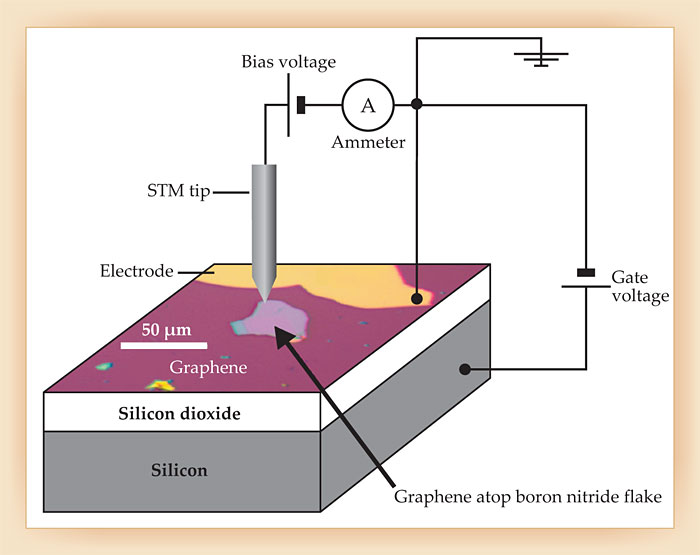
Levitov’s calculations suggested that atomic collapse in graphene should reveal itself as a telltale electronic resonance—a short-lived, quasi-bound electronic state whose energy lies near the Dirac point, the point in energy–momentum space where graphene’s conduction and valence bands meet. Crommie’s lab specializes in making precision scanning tunneling microscopy measurements, which can reveal such resonances. In a typical experimental setup, 3 depicted in figure 1, a bias voltage V is applied between a graphene monolayer and an STM tip. By measuring how the tunneling current I varies with V, the researchers can piece together a picture of how the charge-carrier concentration in the graphene monolayer varies with energy and location. A gate electrode allows the team to manipulate the level of electron or hole doping in the sample. To improve the uniformity of the background charge distribution, the team deposits their graphene samples atop boron nitride flakes.

Figure 1. A scanning tunneling microscopy (STM) setup used to measure graphene’s local density of states. The monolayer graphene sample (purple) is deposited atop flakes of boron nitride to improve the uniformity of the background charge distribution. From variations in the measured current as a function of bias voltage, one can infer the sample’s local density of states. When the graphene is configured atop silicon dioxide and silicon sublayers, its charge-carrier doping can be manipulated with a gate voltage. (Adapted from ref.
Although able to detect even the most subtle electronic hints of atomic collapse, the researchers still faced the nontrivial task of creating an impurity of sufficient charge to see the effect. In principle, a single adsorbed atom with charge +e should lie at or near the predicted threshold for atomic collapse. But in practice, that charge is heavily screened by the electrons in the boron nitride substrate. “Reaching the critical charge threshold turned out to be harder than we thought,” Crommie says. “It became obvious that we’d need to collect several charge impurities together.”
There, too, the team encountered a stumbling block. Single-atom impurities tend to nestle into the potential wells of the graphene hexagons, so once they’ve latched onto the material’s surface, they can’t always be easily repositioned. That was the case for calcium atoms, an otherwise promising form of charge impurity that the team used in early trials. Eventually, the researchers figured out that by heating the Ca impurities they could get the atoms to form movable dimers. Crommie’s students Yang Wang and Dillon Wong devised a way to use an STM tip to nudge the dimers into clusters of as many as five; each dimer carries a charge of +e, so in essence, the team was able to build the charge-impurity equivalent of a boron nucleus.
A five-dimer cluster turned out to be more than sufficient to see atomic collapse. As illustrated by the orange curve in figure 2a, STM spectra collected with the tip positioned far away from such a cluster are typical of what one would find in the absence of impurities. (The quantity dI/dV plotted in the figure roughly corresponds to the charge-carrier local density of states.) The spectrum has the expected minimum at the Dirac point—where, in principle, the material should be free of charge carriers. The increases in the local density of states above and below the Dirac point reflect the introduction of conduction-band electrons and the formation of holes, respectively. The Dirac point is shifted from V = 0 due to an applied gate voltage that prepopulates the sample with holes; the bandgap-like feature, roughly 0.2 eV wide and centered at V = 0, is an artifact of phonon-assisted tunneling.

Figure 2. Atomic collapse in graphene. (a) A resonance (indicated by the red arrow) just below the voltage corresponding to the so-called Dirac point indicates the onset of collapse. (Here, dI/dV, the change in tunneling current with respect to bias voltage V, reflects the electronic local density of states; the bandgap-like feature centered at V = 0 is an artifact of phonon-assisted tunneling.) Spectra were collected with a scanning tunneling microscopy tip at varying distances from a cluster of five positively charged calcium dimers. The resonance, indicative of a short-lived bound electronic state, appears at distances less than about 10 nm. (b) In a spatial map of the resonance intensity, the localized bound state is visible as an orange halo. (Adapted from ref.
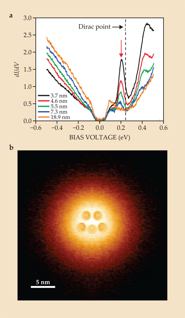
Unlike spectra collected far from the cluster, those collected with the tip positioned within about 10 nm of the dimers exhibit a sharp resonance at V just below the Dirac point and show hints of further oscillations at higher V. The sharp resonance corresponds to the predicted quasi-bound electronic state—the quantum mechanical equivalent of a classical, spiral trajectory toward the charge impurity. In the spatial map of the resonance’s intensity shown in figure 2b, that quasi-bound state is visible as an orange halo surrounding the five Ca dimers.
“Very few labs in the world could have pulled this off,” comments Castro Neto. “From the perspective of new physics, this is one of the most important graphene experiments since the 2005 measurement of the quantum Hall effect.”
Going small, thinking big
Besides potentially shedding light on fundamental questions regarding the stability of matter, the discovery that modestly charged impurities can produce exotic electronic states in graphene has implications for the miniaturization of graphene-based electronics. Conceivably, a tiny gate electrode, shrunk down to nanoscale proportions and charged by an external power source, could give rise to atomic-collapse states like those seen by Crommie and company.
Eventually, researchers may be able to harness that effect. “By understanding and manipulating the atomic-collapse states,” Crommie says, “it may be possible in the future to create new types of device functionality at the nanoscale, similar to quantum dots and transistor-like behaviors.” As for what’s next, Crommie and his coworkers plan to construct lattices of charged impurities to study how atomic-collapse states interact with one another.
References
1. Y. Wang, et al., Science (in press). https://doi.org/10.1126/science.1234320
2. A. V. Shytov, M. I. Katsnelson, L. S. Levitov, Phys. Rev. Lett. 99, 246802 (2007); https://doi.org/10.1103/PhysRevLett.99.246802
V. M. Pereira, J. Nilsson, A. H. Castro Neto, Phys. Rev. Lett. 99, 166802 (2007). https://doi.org/10.1103/PhysRevLett.99.1668023. R. Decker et al., Nano Lett. 11, 2291 (2011).https://doi.org/10.1021/nl2005115


