Graphene photodetectors get gain
DOI: 10.1063/PT.3.1628
Graphene makes for a nearly ideal photodetector: It absorbs light over a broad range of wavelengths—from the UV to the far-IR—and then ballistically conducts the photoexcited electrons, even at room temperature. But as a single monolayer of atoms, graphene can only absorb 2.3% of incident light.
Ever since IBM’s Phaedon Avouris and colleagues demonstrated an ultrafast graphene photodetector three years ago, 1 his group and others have been developing strategies to ameliorate the limited absorption. One can, for instance, place graphene in an optical cavity to repeatedly pass light through it or position plasmonic nanostructures near electrodes on opposite sides of the graphene to dramatically amplify the local electric field.
Researchers led by Gerasimos Konstantatos and Frank Koppens at the Institute of Photonic Sciences in Barcelona, Spain, have now developed a fundamentally different approach. They used graphene as an ultrafast charge-transport channel but relegated the light absorption to a roughly 60-nm-thick film of colloidal quantum dots deposited on it. 2 Because the dots can be synthesized with a broad distribution of sizes (and thus bandgaps), they can absorb over a broad spectral range. More significantly, because graphene is sensitive to any electrostatic perturbation close to its surface, the quantum-dot layer acts like a gate that controls the amount of charge flowing through the graphene below it. The combination of the two materials in a circuit provides a gain mechanism that can generate multiple charge carriers for each incident photon.
As proof of concept, the researchers created an ultrahigh-gain phototransistor. To build the device, shown schematically in the figure, they started with a micron-sized flake of graphene peeled from graphite and deposited on silicon dioxide using the now-famous “Scotch tape” method (see PHYSICS TODAY, August 2010, page 15 ). They then sprayed the surface with lead sulfide quantum dots. Lead sulfide was chosen for its ability to absorb strongly in the visible and IR, and the dots were specially prepared with short ligand molecules that bind them to the graphene and efficiently transfer charge to it.

A hybrid graphene phototransistor. Gold electrodes are the source and drain on opposite sides of a graphene flake deposited on a silicon dioxide/silicon wafer and coated with light-absorbing quantum dots made of lead sulfide. Incident light generates electron–hole pairs in the dots. Holes are transferred to the graphene and quickly drift toward the drain under the influence of a voltage VDS, while electrons remain trapped in the PbS. Capacitive coupling between the oppositely charged layers modulates the current, which is amplified by the continual replenishment of holes that flow through graphene during the milliseconds that electrons remain trapped. A back-gate voltage VBG can be adjusted to tune graphene’s charge density and maximize the circuit’s light sensitivity. (Adapted from ref.
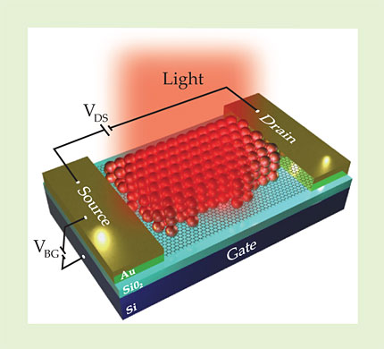
Photons incident on the PbS excite electron–hole pairs. Thanks to an inherent electric field at the graphene–PbS interface, those pairs immediately separate. The electrons migrate outward, only to become trapped for a few hundred milliseconds in shallow surface states, while the holes are swept into the graphene, where in nanoseconds they are conducted under an external field to the drain. Electrons trapped in the PbS dots induce the photogating effect, in which the presence of the electrons alters the graphene’s resistance to current.
The phototransistor’s central feature, its enormous photoconductive gain, can be understood as the ratio of two lifetimes: the electrons’ long lifetime trapped in PbS and the holes’ short lifetime in transit through graphene. The negatively charged quantum dots induce positive carriers in the graphene sheet through capacitive coupling. So under the influence of a bias voltage between the two electrodes, holes are pulled from the source to replace those lost to the drain during the milliseconds that a single electron is trapped. The current through the graphene leads to a measured gain of up to 108 holes per photon. That gain, equivalent to about 107 amps per watt of incident light, is a billion times greater than that of any other graphene-based photodetector.
As a result, signals as small as 10 attowatts are detectable. But such sensitivity comes at the price of slow switching frequencies. Whereas other graphene phototransistors modulate currents at more than 40 GHz (and may potentially exceed 500 GHz), the Barcelona group’s device typically operates at frequencies under 100 Hz. A back-gate voltage, typically used to tune graphene’s change in conductance as additional holes from PbS are transferred, can also act as an electronic shutter. A periodic pulse supplies an electric field that empties the electron traps in the PbS so that the photocurrent through graphene decays and effectively resets the transistor.
“We envision our device as complementary to other graphene-based phototransistors, not as a replacement,” says Koppens. He and Konstantatos imagine that it will find a niche in such applications as visible- and IR-sensitive cameras that can capture images at video rates. Andrea Ferrari of the University of Cambridge regards the achievement as having broader significance. It’s the first, he argues, of a wide variety of sensors that researchers are likely to engineer from the interaction between graphene and quantum dots.
References
1. F. Xia et al., Nat. Nanotechnol. 4, 839 (2009). https://doi.org/10.1038/nnano.2009.292
2. G. Konstantatos et al., Nat. Nanotechnol. 7, 363 (2012).https://doi.org/10.1038/nnano.2012.60


