Discover
/
Article

Diamond nanoneedles turn metallic

NOV 06, 2020
Bending a diamond needle transforms its electronic band structure from that of an insulator to that of a semiconductor or metal.

If you ever manage to deform a diamond, you’re likely to break it. That’s because the hardest natural material on Earth is also inelastic and brittle. Two years ago, Ming Dao (MIT), Subra Suresh (Nanyang Technological University in Singapore), and their collaborators demonstrated that when bulk diamonds are etched into fine, 300-nm-wide needles, they become nearly defect-free. The transformation allows diamonds to elastically bend under the pressure of an indenter tip, as shown in the figure, and withstand extremely large tensile stresses without breaking.
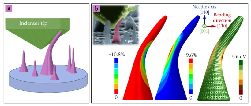
The achievement prompted the researchers to investigate whether the simple process of bending could controllably and reversibly alter the electronic structure of nanocrystal diamond. Teaming up with Ju Li and graduate student Zhe Shi (both at MIT), Dao and Suresh have now followed their earlier study with numerical simulations of the reversible deformation. The team used advanced deep-learning algorithms that reveal the bandgap distributions in nanosized diamond across a range of loading conditions and crystal geometries. The new work confirms that the elastic strain can alter the material’s carbon-bonding configuration enough to close its bandgap from a normally 5.6 eV width as an electrical insulator to 0 eV as a conducting metal. That metallization occurred on the compression side of a bent diamond nanoneedle.

Band engineering using elastic strain is not new. More than two decades ago researchers found applications in microelectronics using engineered strain in silicon. But the strains applied to Si were on the order of 1% or so. According to the new calculations, diamond nanoneedles can be repeatedly exposed to local compressive strains up to −10% on one side and tensile strains above 9% on the other, as shown in the figure—without fracturing or transforming into graphite. The ability to engineer electrical conductivity in diamond without changing its chemical composition or stability opens several specific applications. For example, a tiny piece of bent diamond, with a strain gradient due to bending, could be fashioned into a solar cell or photodetector that captures a range of light frequencies on a single device. Today, that broad-spectrum approach requires layering different materials to take advantage of their different absorption bands. (Z. Shi et al., Proc. Natl. Acad. Sci. USA 117, 24634, 2020 .)

Related content
/
Article
/
Article
The availability of free translation software clinched the decision for the new policy. To some researchers, it’s anathema.
/
Article
The Nancy Grace Roman Space Telescope will survey the sky for vestiges of the universe’s expansion.
/
Article
An ultracold atomic gas can sync into a single quantum state. Researchers uncovered a speed limit for the process that has implications for quantum computing and the evolution of the early universe.

Get PT in your inbox

pt_newsletter_card_blue.png
PT The Week in Physics

A collection of PT's content from the previous week delivered every Monday.

pt_newsletter_card_darkblue.png
PT New Issue Alert

Be notified about the new issue with links to highlights and the full TOC.

pt_newsletter_card_pink.png
PT Webinars & White Papers

The latest webinars, white papers and other informational resources.

By signing up you agree to allow AIP to send you email newsletters. You further agree to our privacy policy and terms of service.