Conductive elastic polymers form the basis for organic skinlike electronics
DOI: 10.1063/1.3001854
Silicon , silicon dioxide, and other materials typically used to make electronic components are intrinsically rigid and brittle. That’s a problem if you want to make a compact device that’s tough, flexible, or both. In principle, you could achieve that goal from stretchy organic materials. The trouble is, suitable insulators and semiconductors exist but not conductors.
The best commercially available conducting elastomers—rubbers filled with graphite particles—have a conductivity of 0.1 siemens per centimeter, high enough for them to work as antistatic sheets but not as elastic wires in integrated circuits. Silver flakes embedded in the rubber can also turn it conductive. But oxidation of the metal particles, electromigration, and a tendency for the conductivity to plummet when the particles separate under stretching make that approach also unsuitable.
To avoid those difficulties, some researchers opt to engineer conventional but rigid conductors into effectively stretchable ones. They face their own hurdles: Thin metal films begin to crack at strains of just 1%, and those on flexible substrates can be deformed by only a few percent before losing their conductivity. But pulling on a latex glove, for example, involves deforming material by 10% or more.
Five years ago Princeton University’s Sigurd Wagner and his then postdoc Stéphanie Lacour found a way to bridge the gap without overstraining the lattice. They evaporated gold films onto silicone polydimethylsiloxane. Thanks to its larger coefficient of thermal expansion, the PDMS compresses the thin metal layer so that it buckles as both cool. Stretchability thus arises from slack added to the film in the form of built-in compressive strain (see Physics Today, July 2003, page 26 ). Wagner and colleagues could then use the films as flexible interconnects that link small rigid device islands.
John Rogers (University of Illinois at Urbana-Champaign) and colleagues have extended Wagner’s approach. Earlier this year they used a transferprinting technique to deposit Si-CMOS circuits onto ultrathin plastic that can be compressed by bonding it to prestrained PDMS. 1 When the PDMS springs back to its original shape, the thin circuits crumple into complex, wavy patterns (see Physics Today, May 2008, page 84 ). The resulting sheet, just 1.2 μ thick, can be twisted, wrapped around the edge of a microscope cover slip, or stretched into arbitrary shapes.
The technology is already spawning intriguing devices, among them a hemispherical camera sensor based on a 16 × 16 array of silicon photodetectors, diodes, and gold interconnects—in essence, an artificial retina. The circuit tolerates elastic strain as high as 50% with negligible effect on its behavior. 2
Polymer solution
As work on stretchable silicon and metallic interconnects has matured, other researchers have continued wrestling with organic materials. Now, the University of Tokyo’s Takao Someya and colleagues have solved the conduction problem by embedding carbon nanotubes in a flexible copolymer. The resulting compound is chemically stable, has a conductivity of 57 S/cm—some 500 times greater than that of graphite-filled rubbers—and can be stretched up to 134% without suffering mechanical damage.
What’s more, the researchers have used the material to connect arrays of thin-film transistors in a two-dimensional elastic matrix and fabricated a device made entirely of organics. 3 The appeal of the work, comments Rogers, lies in the researchers’ materials-based approach: “They’ve synthesized a new conductor that is intrinsically stretchable, rather than implementing structural configurations of known materials.”
Two discoveries led to the successful synthesis. Previous efforts to embed nanotubes into polymers were plagued by the natural tendency of the nanotubes to clump into heavily entangled and stiff bundles because of attractive van der Waals interactions between the tubes. The tendency rendered the nanotube-doped polymers hard and unstretchable. Someya’s colleagues Takanori Fukushima and Takuzo Aida found that mixing the nanotubes with an ionic liquid would neutralize the mutual attractions and create much finer and more numerous bundles. When the resulting “bucky gel” was then blended with a compatible fluorinated copolymer, the nanotubes became dispersed uniformly throughout the polymer without sacrificing its flexibility.
The other key breakthrough came from Kenji Hata (National Institute of Advanced Industrial Science and Technology in Tsukuba, Japan) and coworkers, who developed a method to grow dense forests of single-wall nanotubes with enormous aspect ratios (each 1 mm in length by 3 nm in diameter). Someya and company explain that strands of those “supergrowth” nanotubes, when finely dispersed (and likely broken) by the ionic liquid and blended into the copolymer, remain cross-linked enough that the bulk conductivity is only modestly affected when the film is stretched.
To create elastic wires, Someya’s group cut the polymer film into thin strips, dipped the strips in PDMS for mechanical stability, and punched holes in them. The process gives the wires a fishnet-shaped structure, much like a thin stocking, that increases their elasticity. They could be stretched over 100% for several cycles. Even at such high strains the conductivity exceeded that of graphite-doped rubbers by an order of magnitude. Continued stretching, however, irreversibly lowered the wires’ conductivity.
Applications
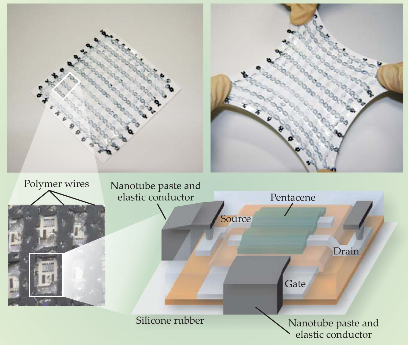
Someya’s team fashioned transistor arrays such as the one pictured on page 18 as proof of principle for the material’s electronics suitability. Contact points between stretchable and rigid materials are particularly prone to breaking. To minimize the problem, the team also synthesized an adhesive paste, again using a recipe that combined the ionic liquid, ultralong nanotubes, and a copolymer. But instead of turning the nanotube dispersion into thin, holey PDMS-coated wires, they allowed it to air dry into an elastic compound that could glue the rigid transistor contact pads to the elastic wires. Even when the two-dimensional matrix is stretched by as much as 70%, the electrical characterisitics of the transistors remained unchanged, mainly because they are not deformed.

This electronic circuit (top panels) consists of a 10 × 10 array of organic transistors connected by a matrix of conducting polymer wires doped with single-wall carbon nanotubes. Coated in white silicone rubber, the matrix can be stretched up to 70% without affecting its electrical or mechanical properties. The rows and columns of black elastic wires, better visible in the enlargement (bottom left), attach to the gate and source contacts of each pentacene transistor through a conducting paste, also synthesized from nanotubes. The schematic illustrates the connections. Such a transistor array could drive pixels in a display.
(Adapted from ref. 3.)
Someya envisions applications that include inexpensive artificial skins whose temperature- and pressure-sensitive transducers could endow a robot’s hand with the capability of gentle touch. Thin electronic patches could also cover the curved surfaces of a display screen, automotive windshield, or airplane wing.
But the applications can be even more exotic. Rogers’s Illinois team, for example, is working with neurosurgeons to develop implantable circuitry that conforms to the rippled geometry and crevices of the brain—to predict the onset of epileptic seizures, say, or to send in electric pulses that head them off. And in another biomedical experiment, a pig’s heart has been covered in a layer of pressure-sensitive circuitry that can speed or slow its heartbeat on command.
Increasing the integration or pixel density of devices may take some time, though. Meanwhile, efforts are likely to remain more playful—this past month Rogers wrapped a circuit over the dimpled surface of a golfball.
References
1. D.-H. Kim et al., Science 320, 507 (2008).https://doi.org/SCIEAS
10.1126/science.1154367 2. H. C. Ko et al., Nature 454, 748 (2008).https://doi.org/NATUAS
10.1038/nature07113 3. T. Sekitani et al., Science 321, 1468 (2008).https://doi.org/SCIEAS
10.1126/science.1160309


