An atomic-scale optical modulator
DOI: 10.1063/PT.3.3124
Hundreds of electrical transistors can fit in a single square micron on a chip. But the footprint of photonic devices is far from commensurate with that density. Whereas the atom sets the ultimate scaling limit to Moore’s law for electronic components, 1 the minimum size of photonic ones is usually constrained by the diffraction limit of the light waves they handle. For devices that manipulate signals in the IR—the most common wavelength range in telecommunications—that limit is on the scale of microns.
Fortunately, researchers can circumvent the diffraction limit by directing light at the interface between a metal and a dielectric. Doing so induces an interaction between the photons and mobile electrons at the metal’s surface. The interaction excites surface plasmons, charge-density oscillations that propagate along the interface at the same frequency as the light and can readily be channeled into nanometer-scale circuit elements. For the past couple of decades, researchers have been developing the building blocks for such plasmonic circuits: filters, sensors, waveguides, switches, Bragg mirrors, and others (see the article by Thomas Ebbesen, Cyriaque Genet, and Sergey Bozhevolnyi, Physics Today, May 2008, page 44 ).
Exploiting plasmonic interactions, Alexandros Emboras, Juerg Leuthold (both at ETH Zürich), and their colleagues have designed and fabricated an electro-optical modulator that switches an incoming light signal on or off by the movement of at most a few atoms at the end of a sharp tip. 2 No other optical modulator operates at such a small scale.
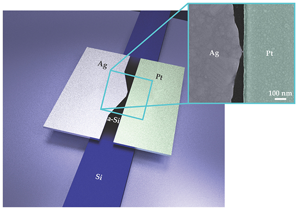
To appreciate how the device works, see figure 1. A silicon waveguide channels an input IR signal into a narrow slot filled with amorphous Si (a-Si) between silver and platinum electrodes. Within the slot, the signal propagates along the metal–insulator boundaries as surface plasmons. Crucially, the slot tapers down to a region an Ag tip juts to within about 20 nm of the Pt. Even a modest voltage applied across the electrodes reversibly pulls Ag cations into the a-Si matrix, where they recombine with electrons from the Pt and form an atomic gap-bridging filament.

Figure 1. An atomic-scale electro-optical modulator consists of a silicon waveguide that channels an IR light beam into a narrow slot, where an insulating layer of amorphous Si (a-Si) covers the waveguide and fills the gap between two metal electrodes, silver and platinum. The slot converts the beam into surface plasmons—oscillations in charge density—that can, under the right conditions, squeeze through the tiniest part of the gap to the opposite side, where they are reconverted into a beam of photons. Increasing or decreasing a voltage applied across the gap builds or breaks a conductive bridge (inset, center) between electrodes and thereby determines whether the IR transmission is on or off. (Adapted from ref.
When the researchers sent a 1550 nm light beam into the waveguide and swept the voltage across the gap from −0.025 V to +1.5 V, they were surprised to find that the output signal intensity abruptly increased by 10 dB as soon as the filament shorted the circuit and current flowed. When they swept the voltage down again, the IR output remained high until the voltage reached a threshold around 0.5 V. At that level, the 1550 nm transmission and the current both turned off, as shown in figure 2a.

Figure 2. Changes in current across the gap between the electrodes in the metal-insulator-metal waveguide (a) were measured in tandem with optical transmission through the waveguide as an applied voltage was swept cyclically up and down. The voltage sweep extends a conductive filament (upward arrow) between electrodes until it shorts the circuit, allowing current to flow, or partially removes it (downward arrow), cutting off conduction. In the off state, the circuit is open and the optical output remains low; in the on state, the circuit is closed and optical output is high. (b) The transmission intensity of a 1550-nm-wavelength beam rises by an order of magnitude when the filament bridges the gap, switching the state from off to on. (Adapted from ref.
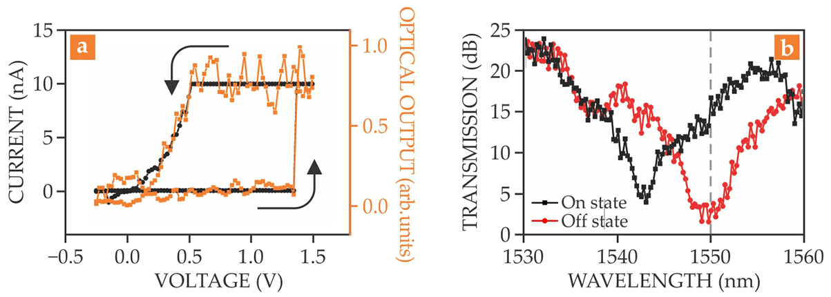
The narrowest section of the waveguide can behave like a resonator. While analyzing the device’s behavior, the group realized that the change in electrical conductance when the filament closes the circuit so alters the local optical properties of the waveguide that the plasmon resonance wavelength blueshifts by nearly 10 nm, as shown in figure 2b.
That shift is attributable to the change in capacitive coupling between the electrodes when the a-Si channel switches between being open and short circuited—the modulator’s off and on states, respectively. In the off state, the light’s 1550 nm wavelength matches the plasmons’ resonance wavelength and almost none of the signal passes through the waveguide: The light’s energy instead excites an oscillating charge dipole across the gap. But once electromigrated atoms bridge the gap, the concomitant change in charge distribution detunes the plasmons’ resonance wavelength far enough away from the propagating 1550-nm wavelength that the light passes through the waveguide relatively unattenuated.
Charge quantization
Although Emboras and his colleagues can’t tell how many atoms actually relocate on each voltage swing, they found quantized levels of conductance, derived from their current–voltage plots, consistent with the relocation of as few as one or two atoms. Indeed, a fully formed bridge isn’t necessary for a working optical switch. Recent theories show that quantum tunneling across a gap can modify the optical response, 3 a result verified four years ago by Jeremy Baumberg (University of Cambridge), Javier Aizpurua (Spanish Council for Physics Research), and their colleagues. 4
Even so, the 10 dB enhancement was a surprise to the researchers. In 2013, while working as a postdoc in Uriel Levy’s group at the Hebrew University of Jerusalem, Emboras had made early versions of the optical modulator; they exhibited a transmission contrast of a scant few percent. 5 When he moved to ETH Zürich, he and his colleagues realized why: In the older work, the Ag layer was parallel to the opposite electrode for hundreds of nanometers at the electrodes’ closest configuration, creating a long enough channel to nucleate and grow multiple filaments at the interfaces, which effectively weakened the optical response. Meanwhile, Leuthold’s group had been working on tightly confining plasmonic modes in a waveguide and achieved high contrast between the on and off transmission states in its own switches. 6 In the new implementation, tapering the Ag electrode to a point ensures the formation of a single filament where the gap is narrowest and the electric field from the voltage driving the electromigration not only is a maximum but is enhanced by the strong confinement of an optical cavity.
According to Harald Giessen, a University of Stuttgart physicist unaffiliated with the new work, one might be able to exploit the large change in plasmon resonance wavelength from the movement of so few atoms to study charge transport optically. But he’s also enthusiastic about the advantageous properties of the new device in the role it was designed for. Besides being tiny, the switch is compatible with CMOS electronics, consumes a mere 12.5 femtojoules per cycle, and can modulate the transmission signal reliably for months in ambient conditions and at rates up to 50 MHz. “An eventually optimized version will certainly be faster,” says Leuthold. “Atoms are so light, there’s no fundamental reason they couldn’t move at terahertz rates.”
References
1. See, for example, K. Terabe et al., Nature 433, 47 (2005). https://doi.org/10.1038/nature03190
2. A. Emboras et al., Nano Lett. 16, 709 (2016). https://doi.org/10.1021/acs.nanolett.5b04537
3. J. Zuloaga, E. Prodan, P. Nordlander, Nano Lett. 9, 887 (2009) https://doi.org/10.1021/nl803811g ; see also
F. Marchesin et al., ACS Photonics 3, 269 (2016). https://doi.org/10.1021/acsphotonics.5b006094. K. J. Savage et al., Nature 491, 574 (2012) https://doi.org/10.1038/nature11653 ; see also
G. Di Martino et al., Small 12, 1334 (2016). https://doi.org/10.1002/smll.2015031655. A. Emboras et al., Nano Lett. 13, 6151 (2013). https://doi.org/10.1021/nl403486x
6. C. Hoessbacher et al., Optica 1, 198 (2014).https://doi.org/10.1364/OPTICA.1.000198


