An all-nanocrystal transistor emerges from solution
DOI: 10.1063/PT.3.3185
The integrated circuits that undergird modern electronics pack billions of transistors into an area smaller than a dime. Undisputed technological marvels though they are, the silicon-based devices—and the conventional methods to make them—aren’t well suited to applications that require large area, ability to flex, or both. Manufacturing plants have to maintain expensive ultraclean environments, and fabrication often involves slow, high-vacuum deposition or high-temperature annealing that limits compatibility with many flexible substrate materials. For large electronic displays, photovoltaic arrays, and devices that are incorporated into clothes, the dearth of cost-effective fabrication methods, not limited real estate, is the main obstacle.
Scientists and engineers envision fabricating electronic devices on large sheets of flexible substrates—plastics, paper, and textiles among others. One scenario is to assemble the devices as the substrate is continuously fed from one large roll to another—much in the way text is printed on newspapers. Manufacturers have already begun to explore roll-to-roll processing—for example, to make solar panels—but device performance still lags behind silicon counterparts. New materials don’t necessarily have to reach the high bar set by single-crystal Si, but they should at least compete with the amorphous or polycrystalline Si that’s commonly used for large-area applications.
Among the mix of potential building blocks are nanometer-sized crystals with tailorable electronic properties. Using standard techniques of the trade, chemists can readily synthesize nanocrystals that are conducting, semiconducting, or insulating. Made into colloidal suspensions, they can be deposited on thin plastic sheets at room temperature without the high vacuum required in conventional semiconductor device fabrication. Nanocrystals should thus be ideal for flexible electronics.
However, finding a good recipe for integrating different nanocrystals, with their often complex and sometimes incompatible chemistries, into a field-effect transistor (FET) or other single device has been elusive. Now a University of Pennsylvania group led by Cherie Kagan and Christopher Murray has fabricated a FET entirely from nanocrystals. 1 Figure 1 shows the group’s FETs assembled on a flexible plastic. The fabrication recipe could set the stage for the cost-effective manufacture of flexible devices based on nanocrystals.

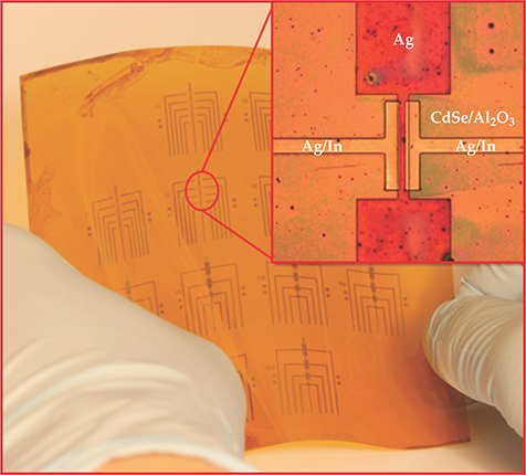
Figure 1. An array of all-nanocrystal field-effect transistors fabricated on Kapton, a commercially available plastic commonly used for printed circuits. The inset shows the details of one FET. The horizontal distance separating the source and drain electrodes (silver/indium) is 30 μm. Viewed here from above, the silver gate electrode is visible although it lies beneath the thin cadmium selenide semiconductor-channel and aluminum oxide insulator layers. (Adapted from ref.
The solution
In essence, a FET is a doped semiconductor channel attached to source and drain electrodes and capacitively coupled to a conducting gate. A voltage applied to the gate controls the current flowing from the source to the drain. For FET performance, the higher the carrier mobility in the semiconducting channel, the better.
Solution-based nanocrystal synthesis uses organic molecules (ligands) that bind to the surfaces of nanocrystals to stabilize them and control their sizes. In a colloidal suspension, the ligands prevent aggregation of the nanocrystals. However, ligands optimized for synthesis often prevent good coupling between particles once they are deposited to form a solid film. Low carrier mobility is the result.
In the 1990s researchers began to find ways to synthesize nanocrystals using one ligand and then swapping it out for another post synthesis. For instance, Ronald Andres and his collaborators at Purdue University showed that the conductivity of a gold-nanocrystal superlattice could be altered through ligand exchange. 2
Then in 2005, while working at the IBM Thomas J. Watson Research Center, Murray and his colleague Dmitri Talapin (now at the University of Chicago) found that post-synthesis replacement of long ligands with compact inorganic molecules boosted the charge mobility in lead selenide nanocrystals. 3 Because of the substitution, they could build FETs using PbSe nanocrystals as the semiconducting channel. Nonetheless, that early success still used single-crystal Si as the substrate, and the semiconducting channel was the only nanocrystal component.
Some assembly required
Researchers have long known that nanocrystals can exhibit tunable properties based on their size, shape, and composition. For example, quantum-confinement effects are routinely exploited in semiconducting nanocrystals, better known as quantum dots, to control their size-dependent bandgaps. Thus, different nanocrystals could be tailored to serve as the different components of a FET. Says Kagan, “We wanted to see if we could design the materials, interfaces, and processes to put the pieces together.”
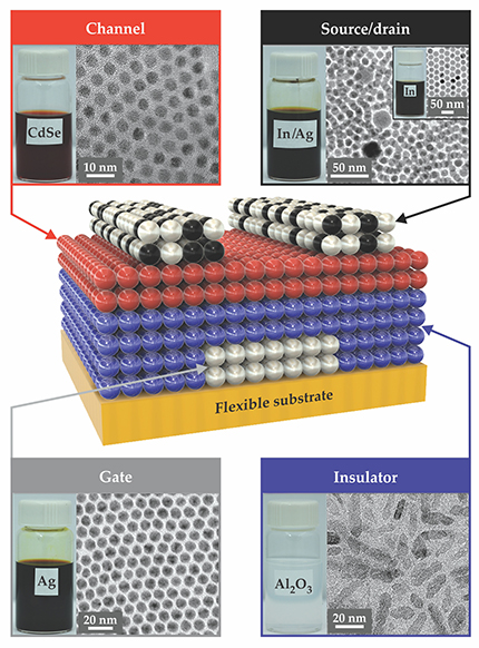
Sounds simple enough, but as Kagan explains, “Just because we have semiconductor, metal, and insulating nanocrystals doesn’t mean we can construct complete devices.” For their all-nanocrystal FETs, the Penn group began with a flexible plastic substrate and sequentially spin-coated each component on top of it: silver for the gate electrode, aluminum oxide for the gate insulator, cadmium selenide for the active semiconductor channel, and a mixture of silver and indium for the source and drain electrodes (see figure 2). The gate, source, and drain electrodes were patterned using photolithography.

Figure 2. The structure of a nanocrystal field-effect transistor. (The spheres in the central schematic are not to scale and do not indicate the actual number of nanocrystal monolayers.) To bypass costly high-vacuum deposition steps, the solution-based fabrication uses colloidal suspensions of nanocrystals for each component. The 80-nm-thick silver gate electrode is insulated from the 60-nm-thick cadmium selenide semiconductor channel by 80 nm of aluminum oxide. The source and drain electrodes are 100 nm thick and made from a mixture of silver and indium nanocrystals. The insets show vials of the suspensions along with transmission electron microscope images that reveal the uniform sizes of the nanocrystals for the channel, gate, source, and drain. (Adapted from ref.
Each step in the process required matching the chemistry between different layers. For instance, to get the positively charged Al2O3 nanocrystals to stick on top of the Ag layer, Kagan and her colleagues had to give the Ag layer’s surface a negative charge through an intermediate treatment with polyelectrolytes. In addition, during the layer-by-layer deposition of Al2O3—in all, Kagan’s group put down three—each layer needed to be similarly treated for the next one to stay on. Fortuitously, the polyelectrolyte treatment turned out to also increase the dielectric constant of the Al2O3 layer, which subsequently enabled the device to operate at a lower voltage.
Once all the layers were assembled, the researchers annealed the device at a modest 250 °C for 10 minutes. Heating freed some of the In atoms from the In nanocrystals to diffuse into the semiconducting CdSe channel. The migration of In atoms into the semiconducting channel made it possible for the group to dope the semiconductor without resorting to a high-vacuum technique such as vapor deposition.
Having demonstrated a working all-nanocrystal FET, Kagan, Murray, and their collaborators are looking to develop some printing technique or other high-throughput manufacturing process to make the device fabrication practical. “Our objective was to build the scientific toolbox for nanocrystal materials integration,” says Kagan. “It is part of the road map of developing the class of nanocrystal materials for devices.”
References
1. J.-H. Choi et al., Science 352, 205 (2016). https://doi.org/10.1126/science.aad0371
2. R. P. Andres et al., Science 273, 1690 (1996). https://doi.org/10.1126/science.273.5282.1690
3. D. V. Talapin, C. B. Murray, Science 310, 86 (2005). https://doi.org/10.1126/science.1116703


