Exploring the nanoworld with atomic force microscopy
DOI: 10.1063/1.2435681
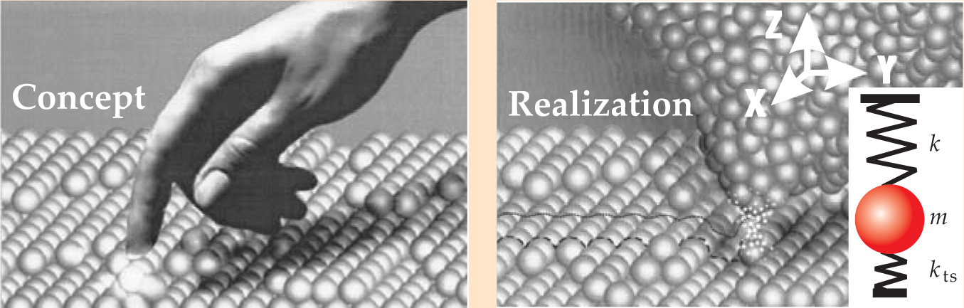
In 1985 Gerd Binnig and Christoph Gerber took a temporary leave from IBM’s Zürich Research Laboratory in Rüschlikon, Switzerland, where the excitement created by the invention of the scanning tunneling microscope (STM) made it hard for them to experiment without frequent interruptions. After relocating to California, they worked with one of us (Quate) and colleagues at Stanford University and with scientists at IBM’s Almaden campus to implement Binnig’s idea of that same year: the atomic force microscope. 1 In February 1986, Binnig, Quate, and Gerber introduced the first prototype AFM, six months before Binnig and Heinrich Rohrer won the Nobel Prize for their STM. The STM records the quantum-mechanical tunneling current that flows between a sharp voltage-biased tip and a conductive surface; from such data one can build a three-dimensional atomic-scale map of the surface. An AFM, in contrast, probes the cumulative forces that act between atoms in the tip and surface (see figure 1).

Figure 1. Like the gentle touch of a tiny finger, the atomic force microscope (AFM) feels the force of atoms on a surface to create an image of the local topography. Mounted on a cantilever having a spring constant k, the tip can be drawn along the surface, while computer-controlled feedback maintains a constant deflection. Or the tip can be deliberately vibrated up and down as it scans a surface. In that dynamic mode, the derivative of the tip–sample force, k ts = dF ts/dz, is measured. As the tip approaches the surface, the AFM senses the shift in the cantilever’s resonance frequency from
(Adapted from G. Binnig, H. Rohrer,
Because forces act among insulators as well as conductors, the idea of force microscopy promised to extend the spatial resolution achieved with an STM. Today, that widespread applicability is reflected in more than 4700 citations of the original 1986 paper, which ranks it among the 10 most-cited articles in Physical Review Letters. This past August the International Conference on Nanoscience and Technology in Basel, Switzerland, celebrated the STM’s 25th anniversary and the AFM’s 20th. The accompanying exhibition hosted more than a dozen manufacturers that offer AFMs for use in ambient conditions, liquid environments, ultrahigh vacuum, and even outer space (aboard the Phoenix Mars mission), plus light and portable versions powered by batteries. Despite the variety of AFM flavors and applications, in this article we will focus on the nature of its atomic-scale imaging.
Path to atomic resolution
The 1986 Binnig, Quate, and Gerber paper reported experimental data of a sapphire surface with lateral features spaced 3 nm apart—far from atomic resolution. But the authors also presented a plethora of visionary ideas on how to improve the AFM’s resolution, including oscillating-cantilever modes that would later become so successful. Their confidence in the potential for atomic-scale imaging—the paper’s central claim—arose partly from the observation of forces acting on the STM tip. But other researchers remained skeptical. Experimental challenges are greater in force microscopy than in tunneling microscopy. Indeed, the STM produced spectacular atomic-scale images shortly after its development (see Quate’s article in Physics Today, August 1986, page 26 , and Tien Tsong’s article in March 2006, page 31 ), but it took a decade for force microscopy to mature into a true atomic-scale tool. 2
The reason lies in the complicated nature of the surface forces that can act on a tip (see
In an AFM, the cumulative force—a mixture of short- and long-range interactions—is much less tractable as a feedback signal. It is not monotonic with distance, nor is measuring forces on the order of nanonewtons with high signal-to-noise ratios an easy task. In vacuum, the force is dominated by attractive van der Waals forces for distances larger than about half a nanometer. Chemical-bonding forces, initially attractive as the tip approaches the surface, turn repulsive as the gap closes.
Forces are usually measured indirectly by determining the deflection of a spring with stiffness k. A force F deflects the cantilever by a distance F/k, and one would think that to obtain a large signal and a good signal-to-noise ratio, soft cantilevers would be best suited. The problem is that large van der Waals forces cause the tip to jump uncontrollably to the surface as the soft, springy cantilever approaches it. To keep a cantilever stable near an attractive sample so that chemical bonds can influence deflection, it turns out that one must either vibrate a soft cantilever with large amplitude or use a stiff cantilever.
Nevertheless, soon after the AFM’s introduction, atomic contrast became apparent in images recorded under ambient conditions. Those images showed periodic lattices without point defects or steps. It soon became clear that the contact area between tip and sample in those experiments must have been much larger than a single atom, and an averaging process was taking place that mimicked true atomic resolution as many tip atoms interacted with many surface atoms. The situation was akin to one egg crate profiling another one.
The key task in achieving true atomic resolution is to single out the chemical-bonding forces of surface atoms on the front atom of the tip from the various other forces at play and exploit its signal for distance feedback. Binnig and Gerber realized that reaching that goal would require a controlled environment—ultrahigh vacuum and low temperature—to cope with the instability problems inherent in the AFM. One of us (Giessibl) joined the project in the newly founded IBM physics group at the University of Munich. After a few years of hard work, atomic resolution on potassium bromide was achieved, but experimental complexities in UHV at helium temperature made operation impractical.
One of Binnig’s graduate students, Frank Ohnesorge, approached the problems associated with cantilever instabilities and strong long-range forces by scanning a calcite crystal under water. 3 There, the van der Waals attraction between tip and water nearly cancels that between tip and sample. The experiment showed an atomically resolved step edge, genuine evidence that the AFM can resolve atoms under water. This capability allowed researchers to image biological samples in vitro.
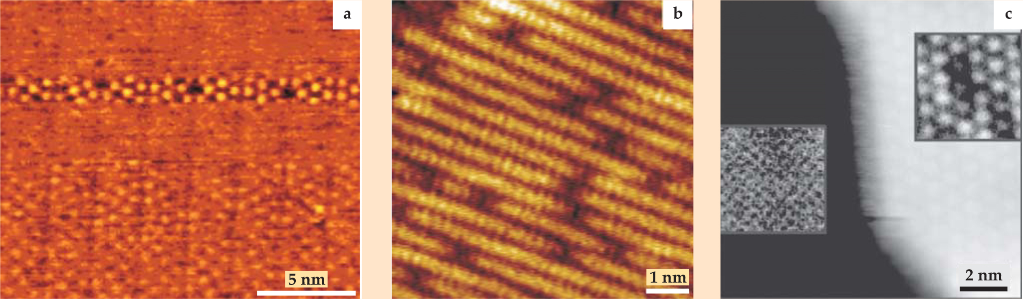
An important cornerstone of atomic-scale imaging remained elusive—an image of the 7 × 7 reconstruction of silicon’s (111) surface. The STM had been quickly embraced by the scientific community partly because of its ability to image that long-enigmatic pattern. Silicon has to be imaged in ultrahigh vacuum, in which the partial compensation of the van der Waals force by a liquid buffer is not possible. Moreover, strong bonds can form between the reactive silicon surface and an imaging tip. In static-mode imaging, those bonds cause severe disruptions of tip and surface atoms.
Dynamic imaging alleviates that problem (see

Figure 2. A gallery of atomic-resolution images, made using the AFM’s frequency-modulation mode of operation. (a) The effect of tip–surface bonding on tip structure accounts for the changes in image contrast in this 1995 scan of the 7 × 7 reconstruction of silicon(111). (b) The oxygen vacancies in titanium oxide are critical to its catalytic activity. Those vacancies appear as dark patches when using an AFM whose tip is positively charged. (c) These images of carbon-60 molecules (right, inset) self-assembled on a layer of potassium bromide (left, inset) demonstrate the AFM’s ability to image atoms and molecules on each side of a step (the central image) that separates the carbon-60 covered regions from the bare KBr surface
((a) ref. 5, Giessibl).
The physics of tip–sample forces
In vacuum, the interaction F ts between the sample and the tip of an atomic force microscope is governed by short-range chemical-bonding forces and long-range van der Waals, electrostatic, and magnetic-dipole forces. The van der Waals forces originate from fluctuations in the electric dipole moment of atoms and their mutual polarization. For two atoms separated by a distance z, the induced dipole–dipole energy varies as 1/z 6. The standard Hamaker approach to calculating the van der Waals energies for macroscopic bodies assumes that individual atom–atom interactions are additive. That makes it possible to calculate the forces acting in simple geometries. For the case of a spherical tip approaching a flat surface, as pictured and plotted here, the van der Waals forces F vdW = −A H R/6z 2, with R being the tip’s radius, A H the Hamaker constant, roughly an electron volt for solids, and z the tip–sample distance.
Electrostatic forces follow the general equation F e = −1/2 U 2dC/dz, where U is the voltage between tip and sample and C the capacitance. For a spherical tip and flat surface, F e = −πε 0 RU 2/z where ε 0 is the permittivity of vacuum.

Both van der Waals and electrostatic interactions can become quite large compared with chemical-bonding forces. A tip of radius 100 nm about 0.5 nm from the surface experiences a van der Waals force of about −10 nN and an electrostatic force of −5.5 nN for U = 1 volt. As modeled by a Morse potential, the chemical bonding energy of two atoms decays exponentially with the distance z until it reaches a repulsive regime. That makes the bonding contribution relevant mainly for tip and surface atoms that are closest to each other. The strong covalent bonds, such as those in silicon, for example, reach maximal attractive forces of about −4 nN.
Topographic imaging
Early research using FM-AFMs focused on atomic resolution of various kinds of surfaces—other semiconductors besides silicon, alkali halides, flourides, titanium, oxides, and metals.
6
Figure
That amplitude may not seem huge, but if one were to magnify a Si atom to the size of an apple, the cantilever would approach the sample atom from as far away as 20 m and the chemical bonding forces responsible for the atomic contrast would act only over the radius of the apple—on the order of centimeters. Thus, the chemical bonding forces affect the motion of the cantilever over a mere 0.2% of the oscillation width.
Researchers tried imaging with smaller amplitude vibrations, but it was difficult to maintain a constant amplitude as the cantilever came close to the sample. The large amplitudes served to stabilize the cantilever in the presence of attractive bonding forces. First, the force that withdraws the cantilever at its turnaround point (kA = 578 nN) is large compared with the chemical bonding force. Second, nonconservative force components that may be present are easily overcome by the large amount of energy stored in the cantilever (E 0 = kA 2/2 = 61 keV). If the tip–sample force is dissipative such that energy δ E is lost during each oscillation cycle, the amplitude fluctuation is given by δA = 1/2 A δ E/E 0 = δ E/(kA). Therefore, stable oscillation at small amplitudes requires stiff cantilevers. The University of Tokyo’s Toyoaki Eguchi and Yukio Hasegawa have found one exception to that rule: 7 Soft cantilevers can be vibrated stably at small amplitudes, provided they have been sharpened by annealing to 900 °C, a process that can dramatically lower the attractive forces.
In the past few years cantilevers have been designed to be hundreds of times stiffer than traditional ones. They have dramatically improved spatial resolution by allowing the tip to stably approach the surface to arbitrarily small distances in the presence of strong forces.
A survey of force-sensing cantilevers
The heart of an AFM is its cantilever, whose deflection toward or away from a surface registers the force of an interaction. Cantilevers can be simple. The first was a hand-crafted, 800-µm strip of gold foil glued to a diamond tip. Soon thereafter, silicon micromachining technology provided cantilevers having tailor-made spring constants and integrated tips, typically composed of silicon nitride or doped silicon. Panel (a) is an example.
To measure the cantilever deflection, the first AFMs used electron tunneling from a scanning tunneling microscope tip placed close to the cantilever. Sensitivity and quiescence were advantages. But the STM can only monitor deflection over a fraction of a nanometer, requires ultrahigh vaccum conditions to work well, and exerts its own complicating force on the cantilever.

Optical methods followed, with two basic types. In beam-bounce detection, a light beam focused on the cantilever deflects in response to any bending of the cantilever. The deflected beam hits a split photodiode, and the ratio of light intensities on the two halves of the photodiode is a measure of the deflection. In interferometric detection, an optical fiber is brought close to the metallized end of a cantilever. Interference between light emitted from the fiber and backscattered light is used to measure the deflection.
Because AFMs use electrical signals to process the image data, electrical-detection methods to monitor deflection have a natural appeal. A cantilever can be designed to exploit the strong piezoresistivity of silicon. The A-shaped cantilever pictured in panel (b) is doped in only the top or bottom half of its thickness. Any deflection strains the conductive layer and changes its electrical resistance. In contrast, piezoelectric devices like the so-called qPlus sensor pictured in panel (c) transform mechanical stress into electrical charge. Oscillations of the cantilever consequently generate an AC current. Because it is difficult to measure the amount of charge created by a constant deflection, piezoelectric detectors are impractical for measuring constant forces. But the frequency and amplitude of the current produced by a vibrating piezoelectric cantilever can be measured with excellent accuracy even at subnanometer amplitudes. Moreover, piezoelectric cantilevers produce a signal that is proportional to frequency. Therefore, the higher harmonics that are created when the cantilever oscillates in an anharmonic potential are naturally amplified.


Aside from its use as a piezoelectric device, what distinguishes the qPlus sensor from the other cantilevers is that it comes virtually ready-made, fashioned out of a quartz tuning fork—the time-keeping element of a consumer watch (panel (c), inset). One need only remove the quartz crystal, strip its metal housing, and supply a sharp tip. Indeed, frequency-modulation AFM and quartz clocks share a common challenge: maintaining high-frequency stability as age, temperature, and other external factors vary. A high Q factor, which conserves battery life in a watch, also reduces frequency noise in an AFM.
Spectroscopy
The initial applications of scanning tunneling microscopy concentrated on topographic imaging, but spectroscopic applications soon surfaced. One method varies the tip–sample distance to measure a metal’s local workfunction φ, the minimum energy required to liberate an electron from a conductive surface. In that approach, dI/dz = −κ I with κ = (2m e φ)1/2/ħ, where m e is the mass of the electron and I the tunneling current. Another method varies the tunneling bias voltage V and records dI/dV, a quantity related to the tip’s and sample’s densities of states.
Both methods are applicable to frequency-modulation force microscopy, in which the frequency shift Δf takes the place of the tunneling current I. The AFM may be configured so that its cantilever swings only close enough to capture the initial stages of bonding. Or it may make and break those bonds during each oscillation cycle. While at the University of Basel in Switzerland, Mark Lantz and colleagues measured the frequency shift as a function of distance over various adatom sites on Si(111)−(7 × 7) and evaluated the bonding strength of individual Si–Si bonds, 8 and Osaka University’s Yoshiaki Sugimoto and colleagues have distinguished adatom species on an alloyed layer of Si and tin on a Si surface by showing that the force between a Si tip atom and a Si sample atom is significantly stronger than the force between a Si tip atom and a Sn sample atom. 8 The techniques used by these groups provide the AFM with chemical specificity.
Toyoko Arai and Masahiko Tomitori (both at the Japan Advanced Institute of Science and Technology in Ishikawa) have found that the bonding force between a Si cantilever tip and a Si surface depends on the bias voltage applied between them. 9 The bias voltage shifts the energy levels of the tip relative to the levels of the sample, and strong interactions occur when maxima in the densities of states as a function of energy overlap in the tip and sample. Choosing an appropriate bias voltage ensures that resonances between tip and sample states occur that lead to strong bonding.
Calculations based on perturbation theory predict that the tunneling current and the tip–sample force are directly related. However, experimental data comparing currents and forces taken simultaneously at small distances suggest that STMs and AFMs actually probe different physical entities and that the images of current and force can exhibit striking inequalities. The STM probes the density of electrons at the Fermi level, while for extremely small tip–sample distances the AFM can be sensitive to electronic states that lie well below the Fermi level. Augsburg University’s Stefan Hembacher and colleagues have shown in simultaneous STM and AFM imaging of graphite at constant height that the AFM sees all surface atoms while the STM sees only the atoms where electrons at the Fermi level are present. 10
While at Stanford University, Ozgur Sahin and coworkers there and in Turkey proposed an AFM method that probes not only the surface topography but also the local stiffness of the sample. In their scheme,
11
one maps the sample topography by imaging in a dynamic mode that holds constant the average interaction force. At the same time, the higher-harmonic motions of the cantilever’s deflection reveal maxima in regions that are very stiff (see
Static and dynamic operating modes
In its simplest form, the AFM is a device whose cantilever tip is held fixed at some constant net repulsive or attractive force. Adopted in the first AFM experiments nearly 20 years ago, this static approach remains in use, though preferentially to image materials under water or other solvents. The drawbacks are that the tip is subject to wear in the repulsive regime, large lateral forces can exist, and absolute-force measurements are noisy.
Dynamically vibrating the cantilever alleviates those problems. In an amplitude-modulation AFM, for instance, the cantilever is driven near its fundamental resonance frequency (typically 20−300 kHz), at which 1/f noise is usually negligible. Its deflections are then monitored by variations in vibration amplitude. Lateral forces are also minimized, because the contact between tip and sample is broken during each vibration cycle. A frequency-modulation AFM suffers even less noise. In an FM-AFM the cantilever oscillates at a fixed amplitude and its frequency is used as a feedback signal.
Imagine a cantilever with stiffness k and effective mass m that vibrates at resonant frequency
The average force gradient is a convolution of the local tip–sample force gradient k ts with a semispherical weight function, computed over the range of distances through which the cantilever oscillates—that is, from z 0 — A to z 0 + A, where z 0 is the undetected tip–sample distance and A the maximum amplitude:
The FM mode requires more sophisticated instrumentation than does amplitude-modulation force microscopy, but the physical observables, frequency shift, and damping are easier to interpret. Moreover, an FM-AFM directly separates dissipative and conservative interaction channels between sample and tip.
To increase the AFM’s short-range sensitivity one must isolate the chemical-bonding component forces from the long-range cumulative forces that act on the tip. The first step is to use frequency modulation over very small amplitudes, because the frequency shift is then proportional to the force gradient. The next step is to exploit a signal that is proportional to a higher-order derivative. Fortunately, small anharmonic components of the cantilever’s motion accompany the frequency shift that occurs as the tip and surface interact; that is, the cantilever’s deflection can be expressed as a sum of its higher harmonic components Σ n≥0 α ncos(n ω t), in which α n refers to the amplitude of the nth harmonic (for n greater than 1):
Typically, the amplitudes of the higher harmonics are about 1% of the base amplitude, but they provide much greater spatial resolution than the frequency shift. As illustrated, the second (green) and third (blue) harmonic components of the deflection are greatly exaggerated.

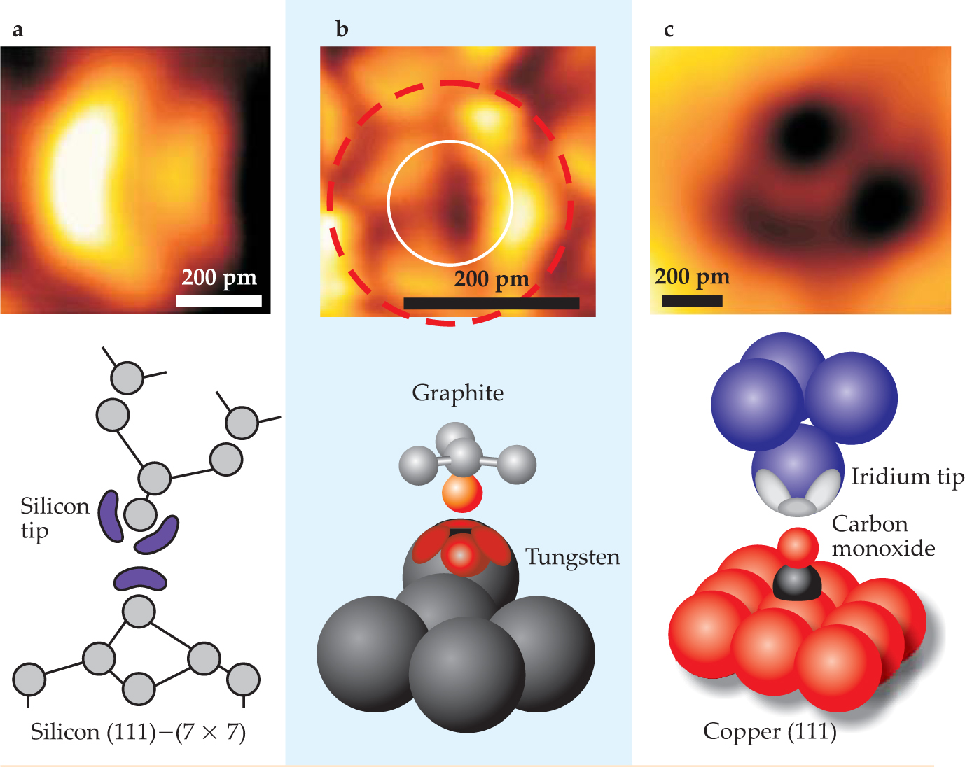
Subatomic imaging
The strength of chemical bonds between atoms is a function of their angular orientation and their distance. Covalent bonds exhibit a strong directional dependence that leads to the formation of molecules and crystals with a characteristic structure. For example, bonds in Si show a tetrahedral symmetry with angles of 109.5°, while the two hydrogen atoms in a water molecule are angled by 107.5°. Not surprisingly the force between an AFM tip and the sample depends not only on their respective chemical identities and the distance between them, but also on the tip atom’s angular orientation with respect to atoms that support it and with respect to atoms on the surface. In the fine details of an AFM image this angular dependence should be apparent as orbital substructures within an atom rather than as simple spheres (see figure 3). 12

Figure 3. Seeing atoms at subatomic resolution using the AFM. Imaging the frequency shift and higher harmonics of an extremely stiff cantilever (1800 N/m) that is restrained to small oscillation amplitudes on the order of a chemical bond can reveal the electronic structure of atoms. (a) In scanning probe microscopy, the surface may also image the tip. As a silicon-atom tip repeatedly vibrates over a silicon surface during a scan, the angular dependence of the bonding force reveals two orbital lobes (blue) of the front silicon tip, the lowermost sp 3 orbital, followed by its more distant (and therefore less pronounced) neighboring orbital.
((b) Adapted from S. Hembacher, F. J. Giessibl, J. Mannhart,
To observe subatomic resolution, the imaging parameters must be optimized. And here is where pushing the cantilever’s stiffness to extremes and oscillating the tip at small amplitudes can help. To appreciate how, consider the effects of large and small oscillations. In large-amplitude FM-AFM imaging, the frequency shift is proportional to F λ 1/2, where F is the force and λ its range. For a total tip–sample force that consists of a long-range force F 1 with range λ 1 and a short range force F s with range λ s, the contribution of the long-range force is 4 times greater than that of the short-range force if F 1 = F s (an optimistic but reasonable assumption using sharp tips) and λ l = 16λ S . In small-amplitude FM-AFM imaging, in contrast, the frequency shift is proportional to the force gradient F/λ, and the long-range contribution is only
Even greater short-range sensitivity is possible by measuring higher-order force gradients in the deflection signal. The van der Waals forces are strong in magnitude, but they vary comparatively little with distance. Chemical forces, in contrast, are weak to intermediate but change very strongly with distance and lateral position. Therefore, by extending the above analysis to the nth-order force gradient, dnF/dzn , one can map out the signal contributions that most reveal the short-range components of the force, since the long-range contribution would be reduced by (λ s/λ l )n.
Stimulated by the work of IBM’s Urs Dürig,
13
who proposed a method to recover the complete tip–sample force from the frequency shift and all higher-harmonic components of the cantilever vibration, scientists at the University of Augsburg found that the higher harmonics of order n can be viewed as a convolution of the nth-order derivative of the force with some weight function. Indeed, they obtained sub-angstrom resolution using this technique to image carbon atoms in a sheet of graphite with a tungsten tip (see figure 3). The tungsten-atom tip properly mapped the graphite lattice, but at each carbon site, a complicated pattern emerged that can be interpreted as a reflection of the charge density of the tungsten atom. In scanning probe microscopy, the probe tip images the surface just as the surface images the probe tip. So if the sample consists of light atoms with small diameters (carbon in this case), the sample can resolve electronic structures in the tip’s front atom. The atomic diameter of carbon is shown as a white circle in figure
STM images of the graphite–tungsten and iridium–carbon monoxide systems recorded simultaneously with the AFM data registered different features. The CO molecule appears as a symmetric dip in an STM image when imaged with small tunneling voltages; none of the internal orbital structure found by the AFM is apparent in STM scans. Similarly, STM imaging of tungsten shows a single symmetric peak.
Atom manipulation
“Putting atoms where we want them” is how Richard Feynman described one of his bold dreams, as outlined in his famous 1959 lecture “There’s plenty of room at the bottom.” 14 In 1990, Donald Eigler and Erhard Schweizer achieved an impressive demonstration of that dream; they used an STM held at 4 K to spell out “IBM” by arranging xenon atoms one at a time on a nickel surface. 15 Indeed, forces that act between the STM tip and the sample can drag individual adatoms along the surface at small tip–surface distances, provided the atoms are weakly bound. Once moved, the atoms can then be imaged by increasing the tip–sample distance.
So far, the STM can pull off such atom manipulation only at low temperatures. But the AFM is not limited by that constraint. Each tip oscillation can exert enough repulsive force to break an atomic bond, for instance, or enough attractive force to influence surface effects, depending on how signal feedback levels are configured. Last year, Morita and his Osaka colleagues created an artificial pattern akin to Eigler’s historic one, but at room temperature. As pictured in figure 4, they found that tin atoms deposited on the (2 × 8) reconstruction of the (111) surface of germanium could be forced to switch positions with Ge atoms. 16

Figure 4. Atom manipulation at room temperature. In contrast to early scanning tunneling microscope images, in which weakly bonded atoms on metallic surfaces were manipulated at low (roughly 4 K) temperatures, the AFM can manipulate strongly bonded atoms that are stable at room temperature. Here, tin atoms sprayed onto the (111) surface of germanium are rearranged to create the chemical symbol Sn.
Properly choosing the scan direction and fine-tuning the tip–surface attractive force can induce that concerted interchange. Such inlays assembled at room temperature remain stable for relatively long periods of time.
Outlook
Another quote from Feynman’s great lecture addresses the service that physicists could render to biologists. As if answering 1950s-era physicists who were advising biologists to use more math to improve their field, Feynman suggested what biology would really need from physics: “What you should do in order for us to make more rapid progress is to make the electron microscope 100 times better.” 14 The AFM has that capacity. Indeed, because the AFM does not rely on the electrical conductivity of specimens to work well, it has found myriad uses in biology (see the article by Carlos Bustamante and David Keller in Physics Today, December 1995, page 32 ).
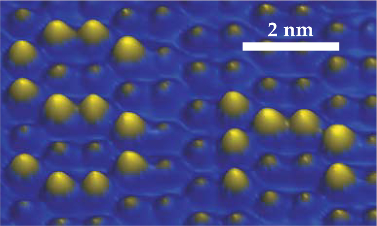
The AFM’s first two decades have seen little overlap between the research of AFM users operating in ambient or liquid environments and that of surface scientists struggling to improve the AFM’s spatial resolution to a level comparable with the STM’s. Lately, this has changed: Two years ago, Hirofumi Yamada’s research group at Kobe University in Japan showed that an FM-AFM can reach molecular and atomic resolution in water and air (see figure 5). 17 What makes the achievement impressive is that most researchers thought that the high Q values that can be achieved for cantilevers oscillating in a vacuum (between about 10 000 and 500 000) were required for frequency measurements of sufficient precision. The Q values of cantilevers oscillating in air and liquid drop to small numbers.

Figure 5. Biological membrane morphology. A frequency-modulation AFM can facilitate the identification of biological structures, in this case a so-called purple membrane—made up of layers of the protein bacteriorhodopsin—on mica, imaged in a phosphate buffer solution. The challenge of frequency-modulated scanning in liquid is to maintain sensitivity despite the low quality factor of the cantilever’s resonance. The clearly resolved molecular scale of the purple membrane and the underlying hexagonal structure of mica (inset) demonstrate that the difficulties are surmountable.
(Courtesy of Hirofumi Yamada.)
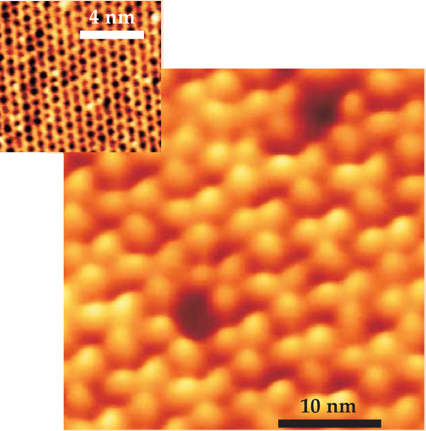
To offset the detrimental effects of ambient environments on the Q values, the Yamada group dramatically reduced the noise associated with their cantilever’s deflection. Specifically, they implemented a new laser-modulation technique to reduce the fluctuations in the output power of light that hits the back of a cantilever. The prospects are good that imaging techniques invented for vacuum will continue to be applicable in ambient or liquid conditions and provide the tools necessary to make progress in fields such as biology and medicine.
With thousands of AFMs in use around the world, it is impossible to capture all important developments in this thriving field. Magnetic-resonance force microscopy, friction-force microscopy, video-rate imaging, and chemical noses that can identify particular species on a surface are just a few of the many other AFM developments that are profoundly affecting nanoscience. 18
We thank Jochen Mannhart and Christoph Gerber for helpful discussions during this article’s preparation.
References
1. G. Binnig, C. F. Quate, C. Gerber, Phys. Rev. Lett. 56, 930 (1986) https://doi.org/10.1103/PhysRevLett.56.930 .
2. S. Morita, R. Wiesendanger, E. Meyer, eds., Noncontact Atomic Force Microscopy, Springer, New York (2002); https://doi.org/10.1007/978-3-642-56019-4
R. Garcia, R. Perez, Surf. Sci. Rep. 47, 197 (2002); https://doi.org/10.1016/S0167-5729(02)00077-8
F. J. Giessibl, Rev. Mod. Phys. 75, 949 (2003) https://doi.org/10.1103/RevModPhys.75.949 .3. F. Ohnesorge, G. Binnig, Science 260, 1451 (1993).
4. T. R. Albrecht et al., J. Appl. Phys. 69, 668 (1991) https://doi.org/10.1063/1.347347 .
5. F. J. Giessibl, Science 267, 68 (1995); https://doi.org/10.1126/science.267.5194.68
S. Kitamura, M. Iwatsuki, Jpn. J. Appl. Phys. 34, L145 (1995) https://doi.org/10.1143/JJAP.34.L145 .6. Y. Sugawara et al., Science 270, 1646 (1995);
A. Schwarz et al., Appl. Surf. Sci. 140, 293 (1999); https://doi.org/10.1016/S0169-4332(98)00543-1
M. Bammerlin et al., Probe Microsc. 1, 3 (1997);
M. Reichling, C. Barth, Phys. Rev. Lett. 83, 768 (1999); https://doi.org/10.1103/PhysRevLett.83.768
K. Fukui, H. Onishi, Y. Iwasawa, Phys. Rev. Lett. 79, 4202 (1997); https://doi.org/10.1103/PhysRevLett.79.4202
J. V. Lauritsen et al.,Nanotechnology 17 , 3436 (2006);
C. Barth, M. Reichling, Nature 414, 54 (2001); https://doi.org/10.1038/35102031
C. Loppacher et al., Phys. Rev. Lett. 90, 066107 (2003); https://doi.org/10.1103/PhysRevLett.90.066107
S. A. Burke et al., Phys. Rev. Lett. 94, 096102 (2005); https://doi.org/10.1103/PhysRevLett.94.096102
C. Loppacher et al., Phys Rev. B 62, 13674 (2000) https://doi.org/10.1103/PhysRevB.62.13674 .7. T. Eguchi, Y. Hasegawa, Phys. Rev. Lett. 89, 266105 (2002) https://doi.org/10.1103/PhysRevLett.89.266105 .
8. M. A. Lantz et al., Science 291, 2580 (2001);
Y. Sugimoto et al., Phys. Rev. B 73, 205329 (2006) https://doi.org/10.1103/PhysRevB.73.205329 .9. T. Arai, M. Tomitori, Phys. Rev. Lett. 93, 256101 (2004).
10. S. Hembacher et al., Proc. Natl. Acad. Sci. USA 100, 12539 (2003).
11. O. Sahin et al., Phys. Rev. B 69, 165416 (2004).
12. F. J. Giessibl et al., Science 289, 422 (2000); https://doi.org/10.1126/science.289.5478.422
H. J. Hug et al., Science 291, 2509 (2001) https://doi.org/10.1126/science.291.5513.2509a .13. U. Dürig, New J. Phys. 2, 5 (2000).
14. R. P. Feynman, The Pleasure of Finding Things Out: The Best Short Works of Richard P. Feynman, Perseus, Cambridge, MA (2000), p. 117.
15. D. Eigler, E. Schweizer, Nature 344, 524 (1990) https://doi.org/10.1038/344524a0 .
16. Y. Sugimoto et al., Nat. Mater. 4, 156 (2005) https://doi.org/10.1038/nmat1297 .
17. T. Fukuma et al., Appl. Phys. Lett. 87, 034101 (2005);
T. Fukuma et al., Rev. Sci. Instrum. 76, 053704 (2005) https://doi.org/10.1063/1.1896938 .18. C. Gerber, H. P. Lang, Nat. Nanotech. 1, 3 (2006) https://doi.org/10.1038/nnano.2006.70 .
More about the authors
Franz Giessibl is a professor of physics at the University of Regensburg and the University of Augsburg in Germany. Calvin Quate is a professor of electrical engineering and applied physics at Stanford University in California.
Franz J. Giessibl, 1 University of Regensburg and the University of Augsburg, Germany .
Calvin F. Quate, 2 Stanford University, California, US .


