Quantum spin Hall effect shows up in a quantum well insulator, just as predicted
DOI: 10.1063/1.2835139
Five years ago, two groups of theorists made a bold proposal: If you apply a voltage to the ends of a semiconducting strip, spin-up electrons will accumulate along one edge, while spin-down electrons will accumulate along the other.
Spin segregation had already been predicted to occur when electrons scatter off impurities, an effect known as the extrinsic spin Hall effect. What made the new proposal intriguing is the mechanism: Under the right conditions, a material’s intrinsic band structure, not its extrinsic impurities, would sort the spins.
Whether this intrinsic spin Hall effect could be observed was controversial. Even in that paragon of purity, epitaxially grown gallium arsenide, scattering seemed likely to smother the effect (see Physics Today, February 2005, page 17 ).
Despite the initial controversy—and perhaps because of it—the two papers set off an explosion of interest in band-based spin flow. Together, the papers have already garnered nearly 2000 citations. Shuichi Murakami and Naoto Nagaosa of the University of Tokyo and Shou-Cheng Zhang of Stanford University wrote one of the papers. 1 The other was by Jairo Sinova of Texas A&M University, Allan MacDonald of the University of Texas at Austin, and their collaborators. 2
Among the ideas the papers spawned was the possibility that the intrinsic spin Hall effect, like the classical Hall effect, has a quantum cousin. The quantum Hall effect shows up when a strong magnetic field is applied to a frigid semiconducting strip. Electrons in the bulk are pinned in cyclotron orbits, but electrons near the edges are free to flow. Provided the sample is pure enough, the conductance G of those edge states is quantized in units of e 2/h.
In 2005 Charles Kane and Eugene Mele of the University of Pennsylvania proposed that graphene would exhibit a quantum spin Hall effect. 3 As in the spin Hall effect, an electric field would cause opposite spins to accumulate on opposite sides, but the electric field would also propel electrons in pairs of quantized counterpropagating edge states.
Now, just two years after it was first proposed, the quantum spin Hall effect has been experimentally confirmed—not in graphene sheets but in quantum wells made from mercury telluride. The speed of the confirmation and its exotic host might seem surprising. But in a 2006 theory paper, Zhang and two of his students, Andrei Bernevig and Taylor Hughes, had provided a recipe for observing the effect in just that system. 4 Within a year, Laurens Molenkamp of the University of Würzburg and his collaborators had built the prescribed wells and found the effect. 5
Spin–orbit coupling
The key ingredient in both the intrinsic and quantum spin Hall effects is spin–orbit coupling. When an electron moves in an electric field, special relativity dictates that it feel a magnetic field in its own frame. The magnetic field couples to the electron’s spin and creates a spin dependence in the band structure. The faster the electron moves, the stronger the coupling.
The quantum spin Hall effect has another key ingredient: a bulk energy gap. In the quantum Hall effect, a strong magnetic field opens a gap as it puts electrons in quantized cyclotron orbits. In the quantum spin Hall effect, the gap is always there: The effect occurs in insulators.
Graphene isn’t ordinarily an insulator. Its conduction and valence bands meet at a point. Kane and Mele realized that spin–orbit coupling would open a small bandgap, thereby turning bulk graphene into an insulator. According to their theory, the coupling would also establish spin-dependent edge states that cross inside the bandgap.
Figure 1 depicts the edge states. Despite appearances, counterpropagating currents do yield a net current. When a longitudinal voltage is applied, more electrons flow in one direction—right, say—than in the other. In figure 1, such a voltage would lead to a conductance of 2e 2/h: e 2/h from the top, blue channel plus e 2/h from the bottom, red channel.

Figure 1. Electronic states have different topologies. In insulators, the outer electrons are pinned by their atoms. A gap is present at all values of momentum. In the quantum Hall regime, a magnetic field pins the outer electrons and opens a gap. The gap is crossed by edge states, which carry current. In the quantum spin Hall regime, a bulk gap is always present. The edge states that cross the gap carry counterpropagating currents of spin-up and spin-down electrons. The three states are topologically distinct. No perturbation can transform one state into another unless it’s strong enough to collapse and reopen the bulk energy gap.
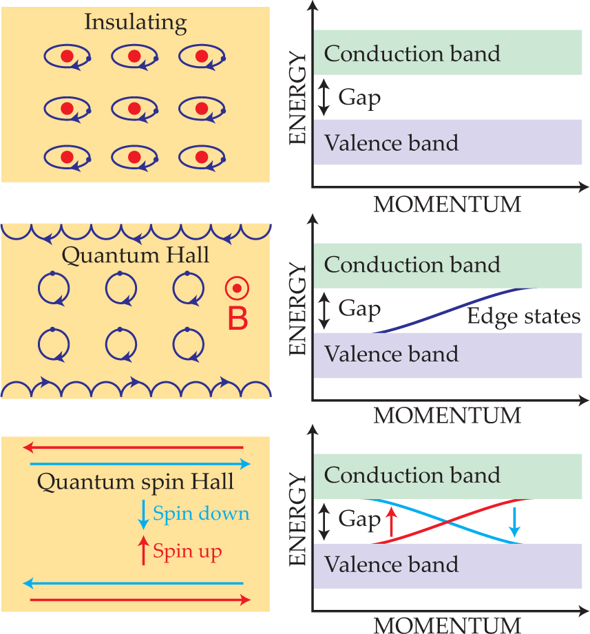
In a second 2005 paper, 6 Kane and Mele showed that graphene isn’t an ordinary insulator. Graphene, unlike silicon dioxide and other insulators, has a nonzero value of a topological invariant called Z2. The edge states obey time-reversal symmetry—that is, reversing the spins and directions of all the electrons leaves the state unchanged. That symmetry, an outcome of the nonzero Z2, makes the edge states particularly robust. To see why, consider figure 1 again.
Suppose a voltage creates a net flow to the right. In principle, there are two ways the rightward conduction could be reduced from its ideal value of 2e 2/h. Spin-down electrons traveling along the top edge (or spin-up electrons traveling along the bottom edge) could scatter into the neighboring, oppositely propagating channel of the opposite spin. But such flips would violate time-reversal symmetry. They don’t occur.
Little energy is needed to scatter an electron into an oppositely propagating channel of the same spin, but those pairs of channels are separated by the insulating bulk of the sample, regardless of sample width.
It turns out that the bandgap in graphene is too small to yield an observable quantum spin Hall effect. Thermally excited electrons can too easily hop across. What material could take its place?
Independently of Kane and Mele, Bernevig and Zhang suggested an alternative: Take a GaAs quantum well and then apply a carefully engineered pressure gradient to create the right, Z2 band structure. 7 Bernevig and Zhang’s proposal, like Kane and Mele’s, is beyond present experimental technology.
The further one gets into the periodic table, the stronger the electric field of the atoms becomes and the faster the outer electrons move. Heavy atoms have strong spin–orbit coupling. That coupling is even stronger if the outer electrons occupy p or other orbitals that have nonzero angular momentum.
One day Zhang was looking at a chart of bandgap versus lattice spacing for semiconducting quantum wells. GaAs, the material in his previous proposal, was there. So too was an oddity. Quantum wells made from HgTe have a negative bandgap: Spin–orbit coupling in HgTe quantum wells is so strong it splits the valence band, which is pre-dominantly p-wave in character, and raises the higher of the split bands above what would otherwise be the s-wave conduction band.
Mercury telluride, Zhang realized, was an ideal material. Moreover, its sister material HgCdTe has a positive bandgap. In a HgCdTe/HgTe/HgCdTe sandwich, the HgTe meat would acquire a positive bandgap once its thickness fell below a certain threshold. Würzburg’s Alexander Pfeuffer-Jeschke had calculated the band structure of HgCdTe/HgTe/HgCdTe sandwiches in 2000 for his PhD thesis. He derived a threshold thickness of 6.3 nm.
The existence of such a threshold is not essential for observing the quantum spin Hall effect. But it does provide a testable prediction: In otherwise identical quantum wells, if you see quantized conductance above the thickness threshold but not below it, the quantum spin Hall effect is the likely culprit.
Mercury telluride
Mercury telluride appears on charts of quantum well bandgaps because the material is used in IR sensors. Defense labs work on the material for night-vision applications, but the presence of mercury makes the material unappealing to work with. Etching and other fabrication steps have to be done at low temperature to avoid mercury turning to liquid.
The University of Würzburg’s Gott-fried Landwehr was not put off. No other semiconducting quantum well has such strong spin–orbit coupling. The prospect of finding novel effects inspired and sustained Landwehr and his colleagues in a 20-year quest to perfect techniques for working with the awkward material. Thanks to those efforts, electron mobility in the cleanest Würzburg crystals now cm stands at 1.5 × 106 cm2 V−1 s−1, just an order of magnitude less than the famed GaAs crystals made at Bell Labs by Loren Pfeiffer and Ken West. When Landwehr retired in 1999, Molenkamp and his collaborator Hartmut Buhmann took over the HgTe project.
Molenkamp first heard about looking for the quantum spin Hall effect in HgTe quantum wells from Zhang in May 2005. At that point, the idea was somewhat abstract. Still, the two agreed to collaborate. The next month Zhang visited Würzburg, where he read Pfeuffer-Jeschke’s thesis. The band-structure calculations were what Zhang needed to make the idea directly testable. By August, he, Bernevig, and Hughes had written up and submitted their HgTe proposal to Science.
Even with two decades of experience of growing HgTe, the Würzburg group still had to develop new lithographic techniques to fabricate quantum wells. Molenkamp and his collaborators found a new photoresist material that could be burned off at the remarkably low temperature of 80 °C.
Gating the quantum well was also a problem. The proposal entails sweeping the Fermi level of the HgTe layer through the bandgap. In principle, the small bandgap of the HgTe quantum well makes the sweep feasible. But in practice, it’s hard to put enough voltage across such a soft material. Molenkamp found that depositing a layer of silicon nitride between the HgCdTe and the gate electrodes did the trick.
Conductance gaps
The basic experiment, shown in figure 2, features a Hall bar of length L and width W, with a central HgTe layer of thickness d. Markus König, a graduate student in the Würzburg group, made several different-sized samples to test different aspects of the quantum spin Hall effect.

Figure 2. To see the quantum spin Hall effect, the Würzburg group built several, four-terminal Hall bars. The bar in this image measures 1 × 1 µm2. It’s covered by a gold gate, which appears here as the small central rectangle. The dark blue regions are mercury cadmium telluride. The dark gray regions are exposed portions of the insulating substrate, (Cd,Zn)Te.
(Courtesy of Laurens Molenkamp.)
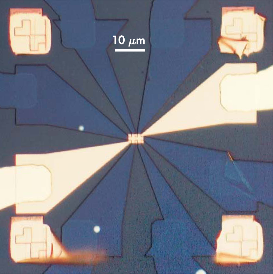
A short enough bar would ensure that longitudinal transport was ballistic, not diffusive, and would give quantized conduction a chance to be observed. Too long, and inelastic scattering would reduce the conductance from its quantized value. Varying W for the same L would reveal whether the conductance really does proceed along edge states. And varying d would reveal whether the expected effect appeared at all.
Those controls were needed to strengthen the experimental case for the quantum spin Hall effect. Molenkamp and his group were looking for spin-dependent transport without using a spin-sensitive sensor.
Some results of the main experiment appear in figure 3. High negative values of the gate voltage pushed the Fermi level into the s-type valence band. Resistance there was therefore low. High positive values of the gate voltage drew the Fermi level into the p-type conduction band. Resistance was again low. What happened in between, when the Fermi level lay in the bandgap, depended on the thickness of the quantum well.

Figure 3. The quantum spin Hall effect features quantized edge currents. To be sure of seeing them, the Würzburg group gated their device to sweep the Fermi level from the valence band, through the bandgap, and into the conduction band. The black trace comes from a sample whose thickness (d < 6.3 nm) ensures that it behaves like a normal insulator. When the Fermi level lies in the bandgap, resistance is high. The red, green, and blue traces come from samples whose thickness (d > 6.3 nm) ensures that they can carry edge states. Quantization of the conductance G is observed when the sample is shorter than the electrons’ mean free path. That’s the case for the red and green traces but not for the blue trace. (Adapted from ref.

When the quantum well was thinner than the predicted 6.3-nm threshold, the quantum spin Hall effect shouldn’t appear. Resistance duly shot up, as shown by the black trace. When the quantum well was thicker than 6.3 nm, quantized conductance could take place. That condition prevailed in the case of the red and green traces, whose values are identical even though the corresponding samples had two different widths (1.0 µm and 0.5 µm). The blue trace is in the quantum spin Hall regime, but at 20 µm the bar was too long to sustain ballistic transport.
Because the quantum spin Hall effect obeys time reversal symmetry, breaking that symmetry destroys the effect. Molenkamp and his collaborators did just that by applying a strong magnetic field. At a value of the field predicted by Bernevig, Hughes, and Zhang, the system quit the quantum spin Hall regime and joined the quantum Hall regime.
Fractional charge, surface states
Molenkamp plans several more tests. He’d like to use two bars, connected at the middle like the letter H, to see whether the spin currents really do travel all the way along the edges. Measuring the spin directly could involve incorporating spin-sensitive gates. Magnetic impurities would break time-reversal symmetry; introducing them should destroy the effect and provide another test.
Meanwhile, theoretical work continues. Zhang and his coworkers have predicted the effect will occur in another quantum well system: indium arsenide/gallium antimonide. They also predict the existence of fractional charge states of the type first envisioned in single chains of polyacetylene by Wu-Pei Su, Robert Schrieffer, and Alan Heeger. That 1979 prediction caused a stir, but has been hard to verify in the lab. The spatial separation of the spin channels in the quantum spin Hall effect makes for an easier test.
Kane and Mele have also developed their ideas. Even though you need a two-dimensional quantum well to see the quantum spin Hall effect, and even though the effect, however hard to observe, should appear in graphene, the effect is not intrinsically 2D. Kane, Mele, and Kane’s graduate student Liang Fu predict that a 3D lump of the right material should exhibit topologically protected surface states.
The discovery of a new Hall effect has more than academic interest. One goal of spin-based electronics, or spintronics, is to circumvent the resistive heating that occurs when electrons are pushed through ever-smaller transistors, capacitors, and other components. Band-based spin flow is dissipationless by nature.
References
1. S. Murakami, N. Nagaosa, S.-C. Zhang, Science 301, 1348 (2003).https://doi.org/10.1126/science.1087128
2. J. Sinova, D. Culcer, Q. Niu, N. A. Sinitsyn, T. Jungwirth, A. H. MacDonald, Phys. Rev. Lett. 92, 126603 (2004).https://doi.org/10.1103/PhysRevLett.92.126603
3. C. L. Kane, E. J. Mele, Phys. Rev. Lett. 95, 226801 (2005).https://doi.org/10.1103/PhysRevLett.95.226801
4. B. A. Bernevig, T. L. Hughes, S.-C. Zhang, Science 314, 1757 (2006).https://doi.org/10.1126/science.1133734
5. M. König, S. Wiedmann, C. Brüne, A. Roth, H. Buhmann, L. W. Molenkamp, X.-L. Qi, S.-C. Zhang, Science 318, 766 (2007).https://doi.org/10.1126/science.1148047
6. C. L. Kane, E. J. Mele, Phys. Rev. Lett. 95, 146802 (2005).https://doi.org/10.1103/PhysRevLett.95.146802
7. B. A. Bernevig, S.-C. Zhang, Phys. Rev. Lett. 96, 106802 (2006).https://doi.org/10.1103/PhysRevLett.96.106802


