Golden Anniversary for AVS
DOI: 10.1063/1.1629006

AVS: The Science and Technology Society will commemorate 50 years of AVS symposia at the international symposium and exhibition that will run from 2 November through 7 November at the Baltimore Convention Center in Maryland. More than 3000 scientists and engineers will gather to celebrate this anniversary through a rich program of technical and plenary sessions, with both a nod to the past and a look toward the future of vacuum science and related technologies.
In parallel with the technical sessions scheduled, there will be topical conferences and special sessions on a range of topics that include contacts to organic materials, high-k gate dielectrics and devices, homeland security, quantitative surface analysis, sputtering, and biomaterials.
To mark the occasion, a series of special anniversary plenary sessions has also been scheduled. To stimulate debate on the direction science and technology may take in this century, speakers have been asked to anticipate the scientific and technical issues that will be central to future AVS symposia.
Keynote speaker Elwood “Woody” Norris will deliver the symposium plenary lecture on Monday at 12:15 Pm. Norris, chairman and CEO of American Technology Corp, will talk about “Invention and Innovation: Gathering Insights from the Future to Make Life Better.”
Shekhar Borkar, an Intel Fellow who directs circuit research at the company’s microprocessor research lab, is the 50th anniversary keynote speaker. He will give a talk entitled “Delaying ‘Forever’: The Future of Moore’s Law” at 12:15 Pm on Tuesday.
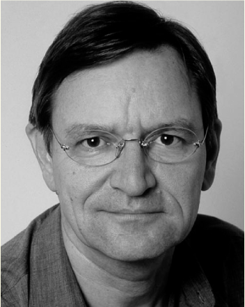
The conference awards assembly will be held at 6:15 Pm on Wednesday. At the ceremony, AVS will present its Medard W. Welch Award to Matthias Scheffler for “developing density functional theory methods to describe surface chemical reactions and enabling their widespread use.” Scheffler directs the theory department at the Fritz Haber Institute in Berlin, Germany.
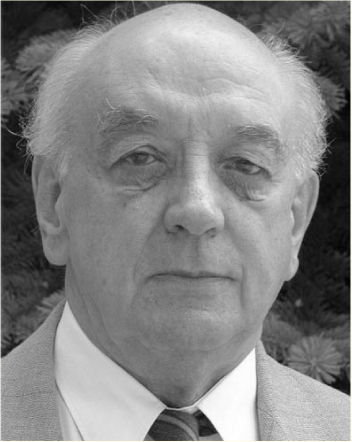
Peter B. Barna will receive the Albert Nerken Award for his “seminal contributions in the use of in situ electron microscopy for the characterization and understanding of microstructural evolution and texture development during thin film growth.” He is a scientific adviser in the Research Institute for Technical Physics and Materials Science at the Hungarian Academy of Sciences in Budapest.
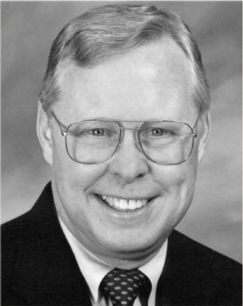
The winner of the John A. Thornton Memorial Award and Lecture is William D. Sproul. He is being honored for his “seminal contributions to the science and technology of sputtering.” Sproul is a senior scientist at Advanced Energy Industries Inc in Fort Collins, Colorado.
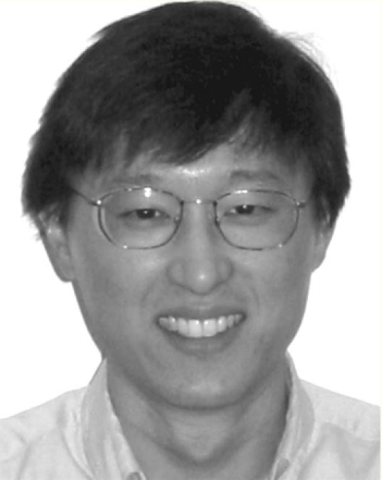
Charles H. Ahn will receive this year’s Peter Mark Memorial Award. Ahn, assistant professor in the applied physics and physics departments at Yale University, is being recognized for “pioneering work on epitaxial complex oxide thin film heterostructures.”
The George T. Hanyo Award will go to Ernest A. Sammann, a research engineer in the Frederick Seitz Materials Research Laboratory at the University of Illinois at Urbana-Champaign. He is being acknowledged for “maintenance, optimization, and development of a suite of complex analytical instruments at peak performance for hundreds of researchers.”
New at the equipment and technology exhibition this year are workshops that will include lectures, demonstrations, and hands-on activities offered by experts from participating companies. The exhibition will be open Tuesday from 11:00 AM to 7:00 Pm, Wednesday from 9:00 AM to 5:00 Pm, and Thursday from 9:00 AM to 3:00 Pm.
For more information about the conference, see http://www.avs.org/symposium/baltimore/default.asp .
Sessions with invited speakers
Sunday, 2 November
Morning
Workshop on sputtering. Berg, De Gryse, Kools
Afternoon
Workshop on sputtering. Petrov, Scholl, Anders, Hopwood
Biomaterials plenary session. Nilsson, Lundstrom, Whitesides
Monday, 3 November
Morning
Protein-surface interactions. Grainger
Looking back: Fifty years of vacuum science and technology. Kornelsen, Redhead, Welch, Hablanian, Dylla
Critical dimension etching. Gottscho
Quantum dots and nanoscale devices. Klimov
Electronic properties of high-k dielectrics and their interfaces. Wilk, Miyazaki
Contacts to molecules and molecular films I. Cahen, Frisbie
Advances in quantitative surface analysis. Castle, Geller, Winograd
Heteroepitaxy of wide-bandgap semiconductors. Doolittle
Modern challenges in surface engineering. Robertson, Harrison, Cui, Schneider, Sproul
Practical surface science. Burrell
Gas-surface dynamics. Kay
Catalysis I: Adsorption and reactions of small molecules at surfaces. Scheffler
Surface diffusion and wetting. Swartzentruber
Atomic layer deposition. Ritala, Gordon
Afternoon
Non-fouling surfaces and biolubrication. Kingshott, Spencer
Challenges in advanced materials and new processes for semiconductor manufacturing. Chong, Richardson, Shadman, Xi, Miller
Where next for nanotechnology? Hays, Hu, Tirrell, Tour, Randall
Plasma sources. Chen
MEMS etching. Gianchandani
Magnetic recording and magnetoresistive structures. Minor, Yuasa
High-k dielectric stability. Chang, Stemmer, Garfunkel
Contacts to molecules and molecular films II. Bredas
Thin-film metrology. Brundle, Seah
Defects and interfaces in electronic materials and devices. Bradley, Rosenwaks
Hard coatings: Preparation, properties, wear, and nanotribology. Vlcek
Stimulated processes at surfaces. McFarland
Tribology, adhesion, and friction. Israelachvili
Structure and reactivity of metal clusters. Goodman
Atomic layer deposition and low-k. Rossnagel, Travaly
Tuesday, 4 November
Morning
Cell/surface interactions. Garcia, Dufrene
Nanowires. Yang
Packaging and role of interface engineering in IC processing. Hosack, Ho, Kelber, Suo, Murali
Information. Cremer, Craighead, Simmons, Goldstein, Stormer
Plasma diagnostics: Processing. Donnelly
Plasma-enhanced chemical vapor deposition. Schmitt, Shiratani
Magnetic imaging and magnetic spectroscopies. Smith, Schneider, Gamelin
High-k dielectric growth and processing. Bersuker
Molecular and organic films and devices: Electronics. Sirringhaus, Bao
Development and characterization of MEMS and NEMS materials. Butler
Narrow-gap semiconductors. Bennett, Chen, Schaff
Nanostructured, nanocomposite, and functionally gradient coatings. Mitterer
Water at interfaces I: Structure and electrochemistry. Searson, Schlossman
Catalysis II: Hydrocarbons at metal surfaces. Zaera
Nucleation and growth. Reutt-Robey
Thin films on organic, polymeric, and biological substrates. Jackson, Dibbs
Afternoon
Nanoscale patterning and lithography. McClelland, Guarini
Directions in semiconductor device scaling for the next decade. Puhakka, Wisnieff, Trybula, Nishi, Huff
Electronic materials. Tu, Van de Walle, Holloway Harper
Dielectric etch. Dalton
Self-assembly and nanomagnetism. Farle, Ross
High-k dielectric characterization. Stesmans, Cartier
Molecular and organic films and devices: Optoelectronics. Duggal, Ballato
Fabrication and characterization of MEMS devices. Livermore
Compound semiconductor growth and processing. Creighton
High-temperature protective coatings. Inspektor
Biomaterials characterization. Beebe Jr
Water at interfaces II: Adsorbed layers. Feibelman, Salmeron
Surfaces and interfaces of semiconductors and compound materials. Osterwalder
Organic functionalization of semiconductor surfaces. Wayner
Transparent conducting oxides. Wager
Wednesday, 5 November
Morning
Cell interactions with patterned surfaces. Chen
Nanomechanics. Pethica, Jarvis
Homeland security. Mackay Hallowell, Fainberg
Surfaces, processing, and materials. Ertl, Kushner, Craford, Tanaka
Current-induced magnetic switching and excitations. Zangwill, Sun
Bionanoscale analysis: Theory to experiment. Brooks
Molecular electronics. McEuen, Kagan
New frontiers in microsystems: NEMS and BioMEMS. Sekaric, Desai
Multifunctional electronic materials. Ahn, Kirchoefer
Dynamic vacuum systems. Berg
High-k materials interface analysis. Lucovsky
Sensors, metrology, and control. Adomaitis, Boning
Afternoon
Biomolecular surface science and microfluidics. Hitchcock, Manz
Nanotribology. Dickinson
Detection of explosives and other chemicals for homeland security. Swager
Future issues in electronics and optoelectronics. Tsao, Stolka, Flatté, Gossard, Isberg
Mechanisms in plasma-surface interactions, van de Sanden
Atmospheric plasmas and micro discharges. Terashima
Magnetic thin films. Allongue
Properties of carbon nanotubes. Suzuki, Matsumoto, Li
Outgassing and large vacuum systems. Watanabe, Weiss
Fuel cell and battery materials/corrosion. Ross, Abraham
Sensors, smart films, and functional materials. Brand, Ullom
Growth and characterization of organic films. Fritz
Perspectives and new opportunities. Duke, Hla, Berndt
Optical thin films and photovoltaics II. Compaan
Thin film-based combinatorial methods. Takeuchi
Thursday, 6 November
Morning
Detection of biological agents and self-cleaning of contaminated surfaces. Petersen, Dordick
Patterned growth and etching of semiconductors. Himpsel
Plasma-surface interactions: Deposition. Arefi-Khonsari
Low-k dielectric etch. Hori
New spintronic materials. Abernathy Bruno
Nanotube growth and processing. Lowndes, Ajayan
Biosensor. Stenger, Kasemo
Development and implementation of sustainable processes. Dornfeld, Chatterjee
Materials for interconnects and contacts to semiconductors. Zhang, Murakami
Reproducibility, precision, and accuracy of vacuum and process measurements. Seidel
Electron spectroscopy. Powell
Heteroepitaxy and strain engineering. Mooney Chason
Catalysis III: High vs. low pressures. Frenken, Nørskov
Oxide structure, growth, and defects. Flavell
Modeling and fundamentals in thin-film deposition. Agarwal, Barnard
Afternoon
Plasma diagnostics: Mechanisms. Klick
Magnetization dynamics. Freeman, Park
Molecular monolayers. Hamers
Biodiagnostics. Breaker, Wightman
Science and technology related to global effects: Emissions, climate, and transport. Shideler, Edmonds
Ferromagnetic and dilute magnetic semiconductors. Zunger, Munekata
Industrial vacuum applications. Mattox, Nemanic
Electron and photon spectroscopies. Zollner, Weightman
In-situ/ex-situ and real-time monitoring. Clarke, Yeadon
Friday, 7 November
Morning
Plasma-surface interactions: Etching. Sawin
Semiconductor spin injection. Hanbicki, Van Dorpe
Nanotechnology and biology. Austin, Gustafsson, Blick
Plasma methods for biointerfaces. Ratner
Low-dimensional structures and amorphous silicon. Noetzel
SIMS. Stevie, Ruedenauer
Mechanical properties of thin films. Vinci


