Electron microscope gets x-ray vision
DOI: 10.1063/PT.3.1290

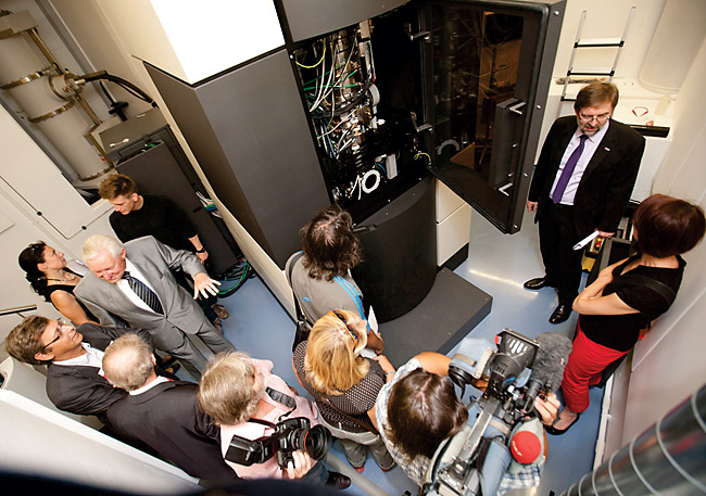
A new electron microscope makes possible direct imaging and identification of individual atoms via x rays. Anticipated applications of the Austrian scanning transmission electron microscope (ASTEM) include analyzing material interfaces and impurities in semiconductor devices, and studying nanoplasmonics. With improved sample preparation methods the instrument could eventually be used to study biomaterials, says Ferdinand Hofer, director of the Austrian Center for Electron Microscopy and Nanoanalysis in Graz, where ASTEM was inaugurated on 22 June.
The electron microscope’s resolution of 70 pm (a picometer is 10–12 meters) is not the world’s best; that distinction goes to a 50-pm-resolution instrument at the National Center for Electron Microscopy in Berkeley, California. What ASTEM does offer, says NCEM director Ulrich Dahmen, is a “highly sensitive, large-angle x-ray detector that puts the instrument at the forefront of fine-probe x-ray spectroscopy.”
In an electron microscope, images are produced via elastic and inelastic interactions of electrons with the sample. In ASTEM, the x rays come from atoms relaxing after core electrons get ejected by incident electrons. Analyzing x rays “has the big advantage that it’s easily possible to detect almost all elements of the periodic table,” says Hofer. “If we see dots that correspond to atoms, we can say if they are sulfur or iron or oxygen.” Understanding chemical composition on the nanoscale is becoming more important, he notes, “because components are shrinking. And we need better resolution to see more details, and the details influence material properties.” ASTEM also opens new possibilities, he adds, by combining x rays with three-dimensional characterization of samples via electron tomography.
Three components give ASTEM its muscle, says Hofer. One is a lens system to correct for image blur caused by spherical aberration. (The Berkeley instrument achieves superior resolution mainly because it also addresses chromatic aberration.) The others are a very bright electron source and a “clever incorporation of x-ray detection,” Hofer says. The detection system is a variation on conventional energy-dispersive x-ray spectroscopy. The electron source and the x-ray detector are proprietary technologies developed by FEI, an electron-microscope company in the Netherlands; the company claims its electron source generates up to 5 times more x rays than other sources and that its wide-angle Super-X system increases collection by a factor of 10. “When we heard about FEI’s x-ray detection system,” Hofer says, “we thought we would cooperate with them. They need the feedback.”
Much of the €4 million (nearly $6 million) tab for ASTEM was shelled out by companies. About one-third of the user time will go to industrial research projects, Hofer says, with the rest for basic science. Raimund Förg, a physicist at the German semiconductor company Infineon, says, “We collaborate with [the Austrian center] because we need a fallback to do high-risk research in a near-industrial atmosphere.”
Förg says Infineon’s first interest in ASTEM is the higher resolution the new instrument offers. But in a few years, he says, he can imagine using the atom-identification aspect of the instrument to look, for example, at interlayers of graphene. “Graphene grows epitaxially, so it’s very important to know the surface. And when you do atomic resolution, you get more information about functionality, and you can influence it.”

The Austrian scanning transmission electron microscope at its unveiling this summer.
AUSTRIAN CENTER FOR ELECTRON MICROSCOPY AND NANOANALYSIS
More about the authors
Toni Feder, tfeder@aip.org


