Diamond’s sparkle is in more than gemstones
DOI: 10.1063/PT.3.4958
Dental implants that can last a lifetime. Robots and particle detectors that can withstand brutal radiation environments. Atomic-scale quantum devices. High-voltage converters that can cut energy losses by 75% in electricity transmission.
Those are a few of manmade diamonds’ cutting-edge applications, not to mention gemstones that are nearly indistinguishable from the natural, far more expensive ones. Diamond cutting and grinding tools have been ubiquitous since the 1950s. Diamond films are now nearing commercial use as coatings for dental, bone, and other surgical implants.
The use of diamond offers clear performance advantages over silicon for high-temperature, high-power, and radiation-hard semiconductors. Diamond’s thermal conductivity is about 20 times that of silicon. For the same surface area, diamond can carry 5000 times the current of silicon. For the same thickness, diamond can withstand 30 times the voltage of silicon, says Khaled Driche, chief technology officer of DiamFab, a startup located in Grenoble, France.
But diamond electronics are held back by the size of crystals that can be manufactured. Diamond will also have to compete against silicon carbide, which has become the go-to replacement material for silicon in high-temperature, high-power environments, according to diamond manufacturers, users, and researchers who work with the material.
Monocrystalline and polycrystalline diamonds differ greatly in their properties and applications, but electronic applications generally require single crystals. Where polycrystalline diamond has been used—in power-electronics applications such as 5G, satellite communications, radar, and fiber-optic data communications—it has been to utilize the material’s passive properties, such as unparalleled thermal conductivity and broadband transparency, says Daniel Twitchen, chief technologist at the De Beers Group–owned Element Six.

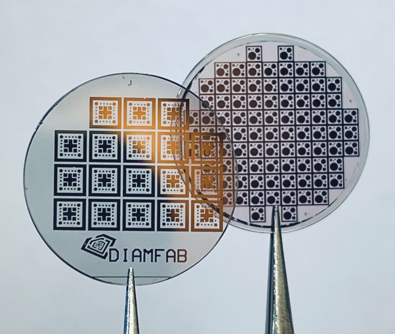
Schottky-diode devices are fabricated by DIAMBFAB, Grenoble, France (left) and MinimalFab, Tsukuba, Japan (right).
DIAMFAB; MINIMALFAB
The two primary techniques of diamond synthesis are high pressure and high temperature (HPHT) and chemical vapor deposition (CVD). First used by the Swedish company Asea in the early 1950s, the HPHT process was kept secret until General Electric claimed the discovery in 1955. Today, metal alloys like iron–nickel, iron–cobalt, and nickel–manganese are used to catalyze diamond growth using graphite in giant anvils at pressures of 5–6 GPa and temperatures of 1300–1600 °C.
A single HPHT system can potentially generate up to a kilogram of diamonds per hour, says Twitchen. The material’s high nitrogen content, around 200 ppm, improves its resistance to cracking, providing performance in machining, grinding, and cutting applications.
In contrast, the CVD process grows diamonds typically in a plasma of hydrogen and methane in a high-vacuum chamber. Carbon atoms are deposited layer upon layer onto diamond substrates known as seeds, which can be supplied from HPHT or CVD. The epitaxially grown diamond maintains the single-crystal structure of the seed.
One millimeter of CVD crystal growth requires two days, says Timothy Grotjohn, an electrical- and computer-engineering professor at Michigan State University and former R&D director of the Fraunhofer USA Center for Coatings and Diamond Technologies. In 2019 Grotjohn founded Great Lakes Crystal Technologies, a producer of diamond substrates for semiconductor electronics. The company is funded by multiple Small Business Innovation Research grants, awarded by various federal agencies, but has yet to make a commercial sale.
“There’s a whole other side of the industry that is using CVD to grow gemstones,” says Grotjohn. “They want to grow 5–6 millimeters, so they can cut a 1–2 carat stone. They will run for hundreds of hours or a couple of weeks.” The requirements for semiconductor grade are stiffer than for gems, he adds, since a diamond will look nice even if it includes a large number of impurities that aren’t desirable in electronic material.
Heat and radiation
In addition to reducing impurities, CVD provides a way to precisely control other elements that are added to the crystal. Most notably, boron and phosphorus dopants impart diamonds with p-type and n-type semiconductor properties. That process has been studied for over a decade by Robert Nemanich, a physicist at Arizona State University, and has led to the grant of a patent to the institution.
Diamond’s capability to work at 500 °C or higher—compared with silicon’s limit of about 200 °C—makes doped diamond ideal for high-temperature electronics, says Nemanich. Such conditions occur in, for example, well logging and drilling, aircraft, and electric vehicles.
Nemanich is an adviser to Advent Diamond, an Arizona State spin-off that’s developing diamond radiation detectors, power electronics, diodes, and other electronic components. The company has won seven Small Business Innovation Research awards, from government agencies including the Departments of Energy and Defense, but it has yet to have commercial sales, says Manpuneet Benipal, the company’s CEO.
Diamond tolerates high-radiation environments. That quality was essential for measuring the neutron flux in the debris from the flooded Fukushima Daiichi nuclear reactors, where a diamond sensor mounted to a small remotely operated submarine probed the submerged sludge. The instrument was able to discriminate neutrons in a high gamma-ray background caused by the presence of radioactive cesium and strontium, says Satoshi Koizumi, who leads the Wide Bandgap Semiconductors Group at Japan’s National Institute for Materials Science.
Diamond radiation detectors in the Large Hadron Collider contributed to discovery of the Higgs boson by monitoring the background signal and beam luminosity in the ATLAS and CMS detectors. Diamond could also be a substitute for neutron detectors based on rare helium-3 that are used at border crossings to guard against the smuggling of fissile materials, says Nemanich.
Nitrogen‒vacancy quantum devices are a growing market for single-crystal diamond. Applications include computing, magnetometry sensors, detectors, and cryptography. To make nitrogen–vacancy devices, nitrogen is added to the ingredients during the CVD process. Typically, electron-beam irradiation displaces some carbon atoms, leaving vacancies in the crystal lattice, Grotjohn says. High-temperature annealing then forces the vacancies to locations immediately adjacent to nitrogen atoms.

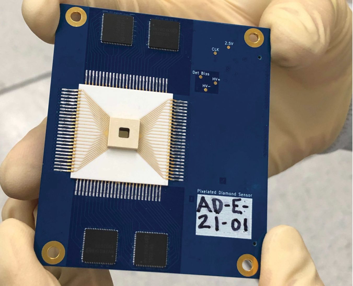
Advent Diamond, an Arizona State University spin-off, fabricated this detector component for x-ray-beam monitoring. The company has been awarded seven Small Business Innovation Research grants, from several federal agencies.
ADVENT DIAMOND
DiamFab is part of an Airbus-led project to make a hybrid aircraft, in which one engine is fully electric and the other is a conventional turbine. Driche says one component will be a power converter based on diamond transistors.
Replacing all the silicon power electronics used in an airliner with diamond components would cut its weight by 1800 kg, Driche says. Such a reduction is possible because diamond devices wouldn’t require the heat dissipators that compose about 80% of the total mass and volume of silicon-based aircraft voltage converters.
Diamond electrodes are used in electrochemical applications such as the destruction of organic wastes that are by-products of chemical processes found in the oil and gas and pharmaceutical industries. They are also used in point-of-use ozone production systems for chemical-free water purification, which are manufactured by companies including Siemens, Condias, and DiaCCon.
Bigger is better
Currently available synthetic single-crystal sizes, typically up to 10 mm, have been sufficient for applications in spectroscopy, Raman lasers, and particle detectors, says Twitchen. Devices that benefit from diamond’s active properties, such as sensing a field or acting as a switch or transistor, remain mostly at the R&D stage.
One thing seems clear: Widespread use of diamond for semiconductors will require larger single-crystal-wafer sizes of at least 50 mm. That’s well beyond today’s state of the art, which are somewhere shy of 25 mm (1 inch). “We are far from being able to fabricate 1-inch substrates with a homogenous crystalline orientation on a commercial basis,” says Philippe Bergonzo, the US representative for Seki Diamond Systems, which makes CVD diamond-synthesis machines.
Twitchen says that there are no fundamental research barriers preventing larger wafer sizes. “The key question here is whether the markets that need this technology will support the engineering costs it will take to scale up.”
Driche says wafers a minimum of 200 mm in size will be needed to compete with silicon in nonniche applications. But he says one company told him that if 150 mm wafers were available, they could use them to fabricate RF devices and next-generation 6G cell phones.
Yet if someone were to make even a high-purity 50 mm single-crystal diamond and replicate it for sale, that producer would be giving away their exclusivity to the buyer, who could use it to grow diamonds of the same size. Bergonzo says it’s unlikely that the originator could obtain intellectual property rights to the process, because a single crystal of similar size may exist in nature.
Etienne Gheeraert, a professor at the University of Grenoble Alpes and researcher at the Néel Institute, headed a European Union–funded project called GreenDiamond to develop a diamond-based high-voltage converter for carrying electricity produced by offshore wind farms. Such converters are expected to become increasingly important as electricity generated by renewable sources of energy is transported over long distances to consumers. Existing silicon-based electronic devices lose as much as 9% of the energy in the conversion process. Although Gheeraert’s project demonstrated that utility-scale diamond voltage converters could reduce those losses to 2%, he says a working device will require 50 mm single-crystal wafers.
Gheeraert expects CVD, HPHT, or both will be capable of producing 50 mm diamond wafers by 2030, but at a cost of $10 000 apiece. An alternative production method is being developed in a project he’s part of that’s sponsored by the French Alternative Energies and Atomic Energy Commission in Saclay. Called Mosaic + Smart Cut, the method could reduce that cost to $1000, he says. In that process CVD single-crystal wafers would be sliced horizontally into multiple wafers. Those new seeds would be abutted into a mosaic pattern, and a single wafer would be grown atop the mosaic. Wafers of 75 mm or more should be attainable, he says. Although those wafers won’t be single crystal, Gheeraert says semiconductor designers can work around the “dead zones” that correspond to the spaces between the substrate crystals.

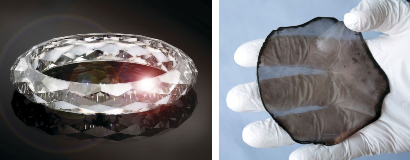
A solid diamond ring (left) was cut by Dutch Diamond Group in Cujik, the Netherlands, from a diamond crystal grown by Audiatec in Augsburg, Germany. That crystal was similar in size to the 92 mm, 155-carat stone (right) that Audiatec produced by ion bombardment of 1-nm-thick carbon on a substrate of iridium.
DUTCH DIAMOND GROUP; MARTIN FISCHER/AUDIATEC
The Smart Cut process was developed by Soitec in France for silicon, and a similar process for diamond was commercialized by the company EDP, located in Japan. The duplication method is used to mass-produce diamonds for sale as seeds and substrates, says Bergonzo, whose company distributes EDP seeds globally. If EDP were to be given a 50 mm single crystal with no impurities and with the same crystalline orientation, it would certainly replicate it. “This would be the biggest breakthrough towards diamond becoming a large-market electronic material,” he says. “But who would give such a primary substrate to EDP? And even if it would exist, if they sold it, at what price?”
Still, developing diamond device technology will require advances not only in diamond material itself but also in the electrical contacts and manufacturing processes, Twitchen says. And for such applications as voltage converters, diamond will have trouble displacing the widely used silicon carbide, which already offers high efficiencies. “The success that silicon carbide is having across a range of industries shows the importance of new semiconductor materials, and there is growing interest in the role diamond might play over the next 10–20 years,” says Twitchen.
A different approach
Matthias Schreck, a physicist at the University of Augsburg in Germany, cofounded Audiatec, which sells diamonds produced by a novel process: Ion-bombardment of a 1-nm-thick carbon layer on a heteroepitaxial (nondiamond) iridium substrate. The company sells its diamonds for use in cutting tools, surgical scalpels, IR optics, and optical windows.
Audiatec has grown single crystals as large as 92 mm and 155 carats (see photo above). Other potential uses are in neutron detection, as host materials for nitrogen–vacancy and other quantum color centers, and in Schottky diodes, Schreck says. Still, he adds, the company continues striving to match the crystal uniformity found in diamond-substrate-grown CVD crystals.
Polycrystalline diamonds are generally used for coatings. Doped polycrystalline grains that are small enough (3–5 nm) can be conducting, says Orlando Auciello, a physicist at the University of Texas at Dallas. He codeveloped “ultrananocrystalline diamond,” a term he has trademarked. The material’s low coefficient of friction, high wear resistance, and biocompatibility have led to applications in seals and bearings for pumps used in drug production and elsewhere.
Auciello’s startup company, Original Biomedical Implants, is currently conducting a clinical trial of diamond-coated dental implants in Mexico. Due to diamond’s chemical inertness, he says, the implants should far outlast today’s widely used but corrosion-prone titanium-aluminum-vanadium alloy. Other potential applications include diamond-coated anodes for lithium-ion batteries that Auciello says will extend cell phone operating time, hydrophilic stents that will prevent blood clotting, and joint implants offering improved wear and biocompatibility.
More about the authors
David Kramer, dkramer@aip.org


