A self-assembled nanopattern exhibits near-perfect order
DOI: 10.1063/PT.3.1460
The fact that microprocessing capability has kept pace with the exponential growth described by Moore’s law, and that data storage capacity has grown at a similar rate, is largely a credit to advances in photolithography. Cutting-edge photolithographic techniques permit device features to be even smaller than the wavelength of the light used to fabricate them. For example, interference effects can be exploited to pattern 50-nm features with UV light. 1 But there’s probably little room left for further cost-effective improvement. It’s inevitable, and perhaps imminent, that Moore’s law and photolithography part ways.
To fashion ever-smaller devices, scientists have looked to make use of molecules that can self-assemble into nanostructures without the help of photochemistry. Diblock copolymers—long-chain molecules made up of two chemically different subunits, joined end to end—are an example (see the article by Frank Bates and Glenn Fredrickson, PHYSICS TODAY, February 1999, page 32 ). In a diblock copolymer made up of polystyrene and polyethylene oxide, for instance, the hydrophobic PS portions tend to huddle together to avoid unfavorable interactions, as do the hydrophilic PEO segments. That localized phase separation creates well-defined, regularly spaced microdomains. Depending on the relative lengths of the PS and PEO segments, the polymer chains might arrange themselves into, say, alternating PS and PEO sheets, PS spheres embedded in a PEO matrix, or, as illustrated in figure 1a, PEO cylinders dispersed in a PS matrix.

Figure 1.Directed self-assembly. (a) To minimize unfavorable interactions, polymer molecules composed of polyethylene oxide (red) and polystyrene (green) may phase separate into cylindrical PEO microdomains embedded in a PS matrix. (b) When the phase separation occurs atop a flat substrate, the PEO microdomains—the wormlike structures in this scanning force microscope image—typically adopt an irregular pattern. (c) But when the microdomains form atop the ridged surface of a nanofaceted sapphire crystal, they assemble into a well-ordered array. The underlying sapphire ridges run parallel to the arrow. (Adapted from ref.
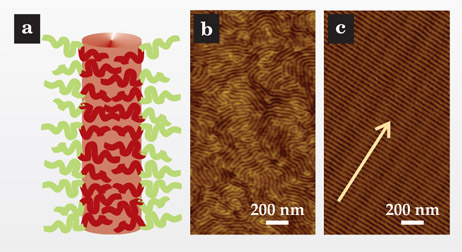
Cylindrical microdomains, in particular, are promising for a number of applications. It’s been demonstrated that they can be chemically etched away to leave behind a nanosieve or replaced with a metal to form nanowires, storage bits, and other miniature device elements. For those elements to be of use for computing or memory storage, however, their arrangement needs to be regular and controllable. As shown in figure 1b, the microdomains that naturally emerge from the self-assembly process don’t form an orderly pattern. Rather, they curve and meander like the ridges of a fingerprint.
One way to get those microdomains to form a regular array is to confine them to a lithographically etched channel. That strategy, however, works only in channels up to a few microns wide. Cylindrical microdomains also coalign under shear, but for very thin films, shearing is cumbersome.
For nearly two decades, Thomas Russell (University of Massachusetts Amherst) has aspired to orchestrate the self-assembly of regular, defect-free nanopatterns without the help of lithography or any kind of external forcing. Such a bottom-up approach would, among other virtues, lend itself to cheap, fast fabrication processes. Now, Russell and an international team of collaborators have succeeded in coercing a 48-nm film of PS–PEO diblock copolymer to arrange into the well-ordered array pictured in figure 1c. 2
In the trenches
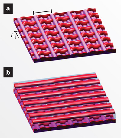
The key element in the team’s breakthrough was a sapphire crystal cut so as to have a thermodynamically unstable surface. When annealed, the surface acquires parallel ridges and trenches. The characteristic trench depth, about 10 nm, happens to be on the order of the diameter of the cylindrical microdomains that naturally form in many phase-separating diblock copolymers.
One might expect that when PS–PEO copolymer is coated onto the sapphire surface to form a bilayer of cylindrical microdomains, the bottommost microdomains would lie along the trenches, like logs in ruts. However, Russell and his colleagues found that all of the microdomains pointed almost perfectly orthogonally to the ridges.
Closer scrutiny of the copolymer and sapphire length scales helps uncover the reason. In the copolymer film, the cylindrical microdomains have a thermodynamically preferred center-to-center spacing L1 of about 30 nm (L1 is a function of the polymer chain length). The spacing λ between ridges on the sapphire surface is typically 35 nm or larger. So for the microdomains to lie along the trenches, they would have to abandon their preferred spacing; polymer chains would be forced to either stretch or contract in a way that increases their potential energy.
To avoid that unfavorable scenario, the bottommost microdomains orient orthogonally to the ridges, as shown in figure 2. Each microdomain in that bottom layer spans only the distance between neighboring ridges. It’s the top layer of cylindrical microdomains—guided into place by the bottom one—that forms the surface-spanning array.

Figure 2.Crossing pattern.(a) When the distance λ between ridges on a sapphire substrate (pink) exceeds the preferred spacing L1 of cylindrical microdomains (red) in an overlying polymer film, the bottommost microdomains align normal to the ridges to minimize free energy. (b) A second layer of microdomains, guided into place by the first, then forms a well-ordered array. (Adapted from ref.
The sapphire substrate, then, is not a template in the strict sense. That is, the self-assembled nanopattern doesn’t mimic or replicate the surface’s spatial features. In particular, the microdomains have nearly perfect alignment, even when the underlying sapphire is marred by defects.
Sampling various locations on a roughly centimeter-sized sample of the nanopatterned film, the team found that the orientation of the ordered cylindrical domains rarely deviates by more than 1° from the mean. Also, grazing-incidence scattering experiments showed distinct Bragg diffraction of x-ray beams incident along the microdomain direction, which suggests that the material’s long-range order is essentially crystalline. Says MIT’s Caroline Ross, “It’s probably the best-ordered pattern one can imagine making with block copolymers.”
In a display of the technique’s versatility, Russell and his colleagues demonstrated that a plastic replica of the nanofaceted sapphire surface performs just fine as a surrogate substrate; the cylindrical domains align as perfectly on the replica as they do on the sapphire. The researchers have also demonstrated that the nanopattern itself can be used to imprint a plastic mold, which could, in turn, serve as a master template in a roll-to-roll printing scheme.
More room at the bottom
Ross thinks the ordered nanopatterns could be useful as extreme-UV or x-ray diffraction gratings. Russell envisions converting them into nanowire arrays or ultradense magnetic storage devices. The patterns’ 30-nm features are already as small as the tiniest features that can be created with photolithography. Can they be made smaller still?
It’s certainly possible to further miniaturize the polymer microdomains. That’s simply a matter of constructing shorter polymer chains. However, as the microdomain length scale shrinks with respect to the ridge spacing of the nanofaceted surface—that is, as L1 becomes much smaller than λ—orientation effects become less important, and so the driving force for microdomain alignment diminishes. Still, Russell is optimistic that his team’s strategy can be used to create ordered patterns with features as small as 3 nm. It’s left to future experiments to prove whether he’s right.
References
1. H. H. Solak et al., Microelectron. Eng. 67-68, 56 (2003). https://doi.org/10.1016/S0167-9317(03)00059-5
2. S. W. Hong, et al., Proc. Natl. Acad. Sci. USA (in press).


