2009 Nobel Prize in Physics honors developments in information technology
DOI: 10.1063/1.3273001
The Royal Swedish Academy of Sciences has chosen to award half of the roughly $1.5 million Nobel Prize in Physics to Charles Kao “for ground-breaking achievements concerning the transmission of light in fibers for optical communication” and the other half to Willard Boyle and George Smith “for the invention of an imaging semiconductor circuit—the CCD sensor.” Average citizens may never have heard of the recipients, but they are almost certainly familiar with the fruits of the laureates’ labor. Optical fibers help deliver signals from around the world to telephones and computers, and charge-coupled devices (CCDs) lie at the heart of most digital cameras. Many have thrilled at the images of astronomical objects taken by CCD cameras aboard satellites such as the Hubble Space Telescope.
All three of the physics Nobelists did their seminal work in telecommunications laboratories nearly 40 years ago, when many industries maintained strong R&D efforts. Kao was working at the former Standard Telecommunications Laboratories, a subsidiary of ITT in Harlow, UK, and Boyle and Smith were at Bell Labs in Murray Hill, New Jersey.
Pointing the way
Born in 1933 in Shanghai, China, Kao had already been working at STL for five years when in 1965 he completed a PhD in electronics engineering at the University of London. By then, telecommunications companies were eagerly searching for ways to transmit greater amounts of information to supply the demand fueled by the growth in the use of televisions and telephones. By the 1960s, researchers were pushing toward high frequencies, which would allow for higher data rates. Effective microwave transmission through the atmosphere, which had been pursued in the 1950s, was limited to frequencies lower than 10 GHz, or wavelengths greater than 3 cm. Researchers thus began looking at millimeter waveguides and at optical waveguides—especially after Theodore Maiman made the first working laser in 1960. Kao was given the responsibility for exploring optical communications at STL.
Scientists had known since the 19th century that light could follow the curves of a water jet or a bent glass rod, guided by total internal reflection—provided the tube has a higher index of refraction than its surroundings. By the 1960s bundles of fibers were used for endoscopic imaging in the human body. Several impediments, however, hindered the use of fibers for transmitting information.
One of those impediments was the dispersion that results from the simultaneous propagation of many transmission modes. Think of each mode as a single ray of light entering the fiber at a given angle. The entry angle determines the zigzag path that the ray will travel. When many modes propagate in a fiber’s core, the signal is distorted by their different propagation speeds. In 1961, Elias Snitzer of American Optical in Massachusetts showed that a fiber with a small enough core (about 3–5 µm) could carry a single waveguide mode. (Multimode transmission later became practical, thanks to the development of cheap LEDs and of multimode fibers having a graded refractive index that reduced modal dispersion.) Kao was excited by the possibility of a single waveguide mode, 1 which would “then have an almost infinite amount of bandwidth.”
Another impediment to optical transmission was the attenuation of light. The absorption of light in the glass fibers of the day was so high–1000 dB/km—that the transmission was limited to a few meters. (One decibel, or dB, is 10 times the log of the power drop, so a factor of 10 power loss gives 10 dB.) Discouraged by the daunting loss of power in fibers then available, researchers like those at STL focused on ways to transmit light through evacuated tubes equipped with lenses, or possibly tubes filled with gas that acted as a lens.
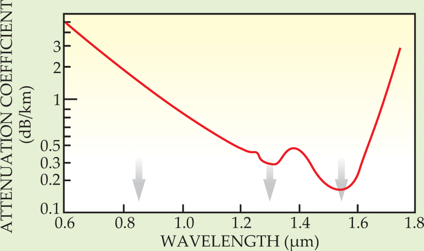
Still, Kao took a closer look at the potential of optical fibers, as opposed to hollow tubes. He realized that losses could be no more than 20 dB/km if fibers were to transmit phone signals for tens of kilometers without repeaters. With George Hockham, he studied both experimentally and theoretically just how much one might reduce the fiber losses. In a 1966 paper, the two researchers reported that the only fundamental limitation on fiber losses, caused by Rayleigh scattering off silica molecules, was on the order of a few decibels per kilometer. 2 Figure 1 shows a loss curve.

Figure 1. Optical fiber loss curve. The attenuation coefficient is determined largely by Rayleigh scattering below 1.2 µm, by hydroxyl radicals around 1.3 m, and by IR absorption at longer wavelengths. Favored wavelengths for telecommunications are indicated by arrows.
(Adapted from ref. 11.)
Kao and Hockham further estimated that the large absorption losses seen in glass fibers of the day were largely caused by transition-metal ion impurities. The researchers concluded that those absorption losses could be reduced below 20 dB/km and that losses due to bending and waveguide imperfections would be small. Similar findings were reported several months later by Alain Werts, then at CSF in France. 3 In subsequent work with other STL colleagues, Kao showed that fused silica (silicon dioxide) had the purity required for optical communication. 4 Recognizing that the cladding had to have a slightly lower index of refraction, Kao proposed using ice for that purpose.
Making the fiber
Kao, along with some researchers in the UK Post Office, which then ran the nation’s telephone system, began campaigning for the development of a low-loss glass fiber made of fused silica. The message got through to some key laboratories.
Robert Maurer of Corning Glass Works in New York recalls that his company heard about fused silica from the UK Post Office around 1966. Fused silica was a challenging material because it has a high melting temperature, but Frank Hyde, working at Corning in the 1940s, had developed a process to make fused silica glass. Maurer recruited Corning’s Donald Keck and Peter Schultz to help make a fiber of silica doped with titanium and having a cladding of pure silica (doping raises the refractive index). Adapting Hyde’s method, Maurer’s team reacted silicon tetrachloride and titanium tetrachloride in a flame and directed the resultant glass particles to the inside of a cylindrical tube. The titanium-doped silica deposited on the tube’s inside wall was then melted and sintered to create a preform from which a thin fiber could be drawn. That method, Schultz notes, permitted precise control of such key properties as glass purity, refractive index, core size, and the quality of the core–cladding interface.
Thanks to the process, Maurer was able to surprise the audience at a 1970 telecommunications conference in London with his announcement of a fiber whose losses were only 16 dB/km. Those first fibers were undesirably weak, but by 1972 the team was making even lower-loss fibers with germanium as the core dopant. Corning also developed a process to deposit the glass from the outside, rather than inside. The outside process proved useful for making multimode fibers having graded refractive index, and later for making singlemode fibers.
At Bell Labs and other major laboratories, early efforts to make optical fibers had focused on purifying conventional silicate glasses. The results from Corning stimulated Bell researchers to look at silica instead.
In 1971, John MacChesney, William French, and Paul O’Connor started using traditional chemical vapor deposition to make high-silica glass fibers doped with germanium. They produced low-loss fibers but at too slow a rate to be practical. They then designed a modified chemical vapor deposition method. In MCVD, chlorides are introduced into a hollow silica glass tube mounted on a lathe that is heated from the outside.
Nanosized particles are deposited on the wall and sintered to pure glass as a torch moves along the outside of the tube. A fiber is subsequently drawn from the collapsed tube. In the ensuing years, MCVD has been adapted to specialty fibers such as erbium-doped amplifiers and polarization-maintaining fibers.
Alan Chynoweth, a former executive director at Bell, credits the late LeGrand Van Uitert for demonstrating a way to make a stable form of boron-doped silica using CVD. In contrast to many other dopants, boron lowered the refractive index of silica, opening the door to prepare optical waveguides with any desired refractive index profile.
In the late 1970s, Tatsuo Izawa and his coworkers at Nippon Telegraph and Telephone Corp in Japan came up with another innovation: the vapor-phase axial deposition method. It is similar to Corning’s outside process but deposition occurs in the vertical rather than lateral direction. The production of telecommunications-grade fiber based on these processes is now routine: The fiber in place today can encircle the globe more than 25 000 times.
In 1970, Kao took a four-year leave of absence at the Chinese University of Hong Kong before returning to STL’s parent company ITT, first in Virginia and later in Connecticut. He became ITT’s corporate director of research in 1986. From 1987 to 1996, Kao served as vice-chancellor at the Chinese University of Hong Kong. He then was CEO of Transtech Services Ltd and of ITX Services. He is now living in Silicon Valley, California.
Charge-coupled devices
As with fiber optics, CCDs grew out of directed research, but the invention soon headed in a different direction from that initially anticipated.
In the late 1960s, Willard Boyle was an executive laboratory director at Bell Labs; his division was involved with semiconductor work. He recalls that the atmosphere at Bell Labs at the time was conducive to fruitful R&D.
Boyle’s boss, Jack Morton, had a division under him that was concerned with developing magnetic bubbles for memory devices. Morton called Boyle one day in 1969 threatening to take money away from the semiconductor work being done under Boyle and put it into the memory-device area—unless Boyle’s division could come up with something to compete with the magnetic bubbles. Boyle still recalls Morton’s penetrating gaze on the screen of the picture phone then in use in the executive offices.
One afternoon shortly thereafter, Boyle met in his office with George Smith, whose department was concerned with silicon diode array camera tubes for picture phones. The two came up with the idea for what they called a charge-coupled array to use bundles of charges rather than magnetic bubbles as carriers of information.
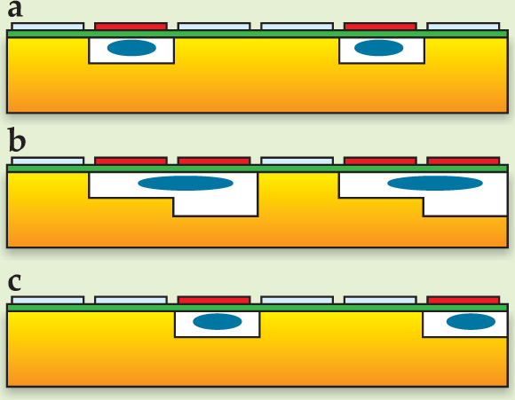
The CCD envisioned by Boyle and Smith is based on metal oxide semiconductor, or MOS, technology. 5 As shown in figure 2, charge can be stored in “puddles” beneath the electrodes of selected MOS capacitors, depending on the electrode charge. Those puddles of charge can be moved from one capacitor to the next by applying a more negative potential to the neighboring electrode. The process is repeated to move charges down the array. In the three-phase design by Boyle and Smith, the presence of the third gate, which remains at its rest potential when the other two are turned on, ensures that charge flows only in one direction.

Figure 2. A CCD consists of an array of metal oxide semiconductor capacitors. Each capacitor consists of a gate electrode (light blue or red according to its potential) atop an n-type silicon substrate (orange), with a thin layer of insulating silicon oxide (green) between. A negative voltage on the gate (red) repels electrons to form a depletion region (white) directly below the gate. (a) Positive charges (blue puddles) are attracted to the depletion region. (b) The charges are moved by applying a more negative voltage to the neighboring gate. (c) After the first gate is turned off, the charge has been transported to the next capacitor.
(Adapted from ref. 11.)
Boyle and Smith noted that a CCD could be used as an imaging device: Incoming light would create an electron-hole pair, with charges being captured in the depletion region and subsequently transferred down the array to a detector. Smith’s immediate supervisor, Eugene Gordon, also suggested using the CCD as a display device.
To demonstrate the viability of the CCD concept, Smith teamed with Gilbert Amelio and Michael Tompsett to build a six-electrode structure and show that the charge could be transferred with minimal loss at high speeds. 6 The three then built an eight-bit shift register by introducing charge at one end of the CCD structure through a forward-biased diode and detecting the charge at the far end by a reverse-biased diode. They reported in 1970 that the shift-register device had a charge-transfer efficiency of 99.9% and transfer times of 2 µs per electrode. 7 They also illustrated the imaging potential by recording the letters “CCD.”
The readout scheme in the CCD is similar to that of a “bucket-brigade device,” a concept for moving charge that had been floating around since 1967. Frederik Sangster and Kees Teer of Philips Research Laboratories Eindhoven, the Netherlands, had proposed in 1969 a bucket-brigade device based on MOS technology. 8 As explained by Smith, however, the Dutch design places a source and drain between each MOS capacitor, thus widening the space between bits and also reducing the efficiency of charge transfer.
Smith recalls 9 that after he and Boyle announced their idea, “Everybody and their uncles started to make inventions based on CCDs.” One of those was the late Dawon Kahng, who, with Martin Atalla, had built the first operative silicon MOS transistor at Bell Labs in 1960. Another was Tompsett, whom Smith credits with doing lots of good work to develop the CCD as an imaging device. Tompsett, who had come to Bell with a background in imaging, patented an idea for reducing the inactive times needed between exposures to read out the charges; that work led to the first area image sensors. Tompsett’s group at Bell worked on making ever larger arrays, replacing metal electrodes with transparent polysilicon ones, and demonstrating a color television at commercial resolution. 10
Ironically, even though CCDs held considerable promise for the two areas of Bell Labs from which it emerged—memory applications and picture phones—the company soon moved out of both areas. Bubble memory and the like couldn’t compete with magnetic hard disks and the random access memory that appeared in the early 1980s. Even earlier, Bell management had concluded that the picture phone was not commercially viable. According to Smith, Bell didn’t have an internal market for any other imaging devices and they could not sell on the open market, so they abandoned CCD research.
Other companies such as Fairchild, Texas Instruments, RCA, and Sony quickly entered the field. Further work on CCDs has introduced the ability to record color images, increased the resolution, and improved the dynamic range. CCD image sensors have found countless applications, including in video and digital cameras, satellite surveillance, and instrumentation for astronomy and astrophysics.
Boyle was born in Amherst, Nova Scotia, Canada, in 1924 and earned a PhD in physics from McGill University in 1950. He retired from Bell Labs in 1979 and returned to his native province. Smith, who was born in White Plains, New York, in 1930, got a PhD in physics from the University of Chicago in 1959. After retiring from Bell Labs in 1986, he spent 17 years sailing around the world before settling down along the New Jersey shore.

Kao

Boyle

Smith
References
1. Oral history: Charles Kao, http://www.ieeeghn.org/wiki/index.php/Oral-History:Charles_Kao (2004).
2. K. C. Kao and G. A. Hockham, Proc. Inst. Electr. Eng. 113, 1151 (1966). https://doi.org/10.1049/piee.1966.0189
3. A. Werts, L’Onde Electr. 46, 967 (1966).
4. J. Hecht, City of Light: The Story of Fiber Optics, Oxford U. Press, New York (2004).
5. W. S. Boyle and G. E. Smith, Bell Sys. Tech. J. 49, 587 (1970).
6. G. F. Amelio, M. F. Tompsett, and G. E. Smith, Bell Sys. Tech. J. 49, 593 (1970).
7. M. F. Tompsett, G. F. Amelio, and G. E. Smith, Appl. Phys. Lett. 17, 111 (1970). https://doi.org/10.1063/1.1653327
8. F. L.J. Sangster and K. Teer, IEEE J. Solid-State Circuits 4, 131 (1969). https://doi.org/10.1109/JSSC.1969.1049975
9. Oral history: George E. Smith, http://www.ieeeghn.org/wiki/index.php/Oral-History:George_E._Smith (2001).
10. M. F. Tompsett, W. J. Bertram, D. A. Sealer, and C. H. Séquin, Electronics 46, 162 (1973).
11. Royal Swedish Academy of Sciences,“Two Revolutionary Optical Technologies,” http://nobelprize.org/nobel_prizes/physics/laureates/2009/sciback_phy_09.pdf .


