Ribbons of micro “houses”
DOI: 10.1063/1.3592019
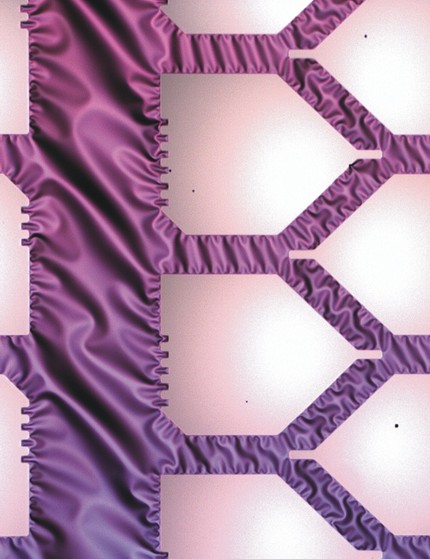
This true-color picture, taken with polarized light in a standard laboratory microscope, shows gallium arsenide patches approximately 400 × 400 μm wide and 3 µm thick (white “house”-shaped objects) connected to one another by only a 50-nm-thick gallium indium phosphide layer (purple). Strained during its growth on a GaAs substrate, the crystalline GaInP layer mechanically relaxes when the substrate is etched off, resulting in the silk-like ripples seen here. Steve Arscott and colleagues at France’s Institute of Electronics, Microelectronics, and Nanotechnology at Université Lille 1 individually removed the GaAs patches and mounted them with microfluidic techniques onto a silica substrate. Daniel Paget and Alistair Rowe at the École Polytechnique used the resulting GaAs cantilevers to study spin-dependent photo-assisted tunneling from the GaAs “chimneys” into magnetized cobalt films. (
To submit candidate images for Back Scatter, visit http://www.physicstoday.org/backscatter.html .

Image by Steve Arscott, submitted by Alistair Rowe.


