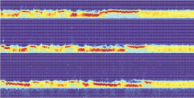
Submicron room-temperature imaging
DOI: 10.1063/1.4797060
Of buried electrical current has been developed. Physicists Gang Xiao and Ben Schrag at Brown University used a magnetoresistance sensor just tens of nanometers across as the basis for their scanning magnetic microscope. By placing the sensor in physical contact with the surface of a current-carrying sample and then rastering continuously, they were able to image the surface magnetic field structure. They then inverted that structure to deduce the current distribution. Shown here is the time development (top to bottom) of electromigration voids (in blue) and hotspots (in red) near the anode of a 3-µm-wide aluminum conductor covered by a 0.1-µm-thick layer of silicon dioxide. (B. D. Schrag, G. Xiao, Appl. Phys. Lett. 82 , 3272, 2003 http://dx.doi.org/10.1063/1.1570499


