Plasma Science, Thin Films, and Nanotech Dominate AVS Symposium
DOI: 10.1063/1.2138424
Do you care about the future of solar power development? Are you curious about the potential applications of structural DNA nanotechnology? Want to know more about gas flow and pump technology?
These topics and scores of others of interest to the vacuum science community are part of the agenda for the 52nd International Symposium of AVS, the Science and Technology Society. This year the five-day annual meeting, which includes an awards ceremony, is slated for Sunday, 30 October, through Friday, 4 November, at the Hynes Convention Center in Boston.
“The Crossbar Architecture for Nanoelectronics” is the topic of this year’s plenary symposium lecture by R. Stanley Williams, an H-P senior fellow at Hewlett-Packard Laboratories in Palo Alto, California. Williams’s talk, at noon Monday in Ballroom A of the convention center, will focus on the “crossbar latch,” a promising nanometer-scale alternative to the transistor. The symposium schedule also includes dozens of lectures, conferences, presentations, and discussions each day. Another highlight is the ASTM Plenary Lecture, which takes place at 2:00pm Sunday in the Hampton Room at the Sheraton Boston Hotel. Susan J. Kerber of Material Interfaces Inc will discuss the application of standards for surface analysis by photon, electron, and ion emission or reflection in manufacturing.
On Wednesday, symposium attendees will gather at 6:15pm in Ballroom A of the convention center for the awards ceremony and reception. Four scientists are being recognized for their accomplishments in the field.
Charles S. Fadley, advanced light source professor for the physics department at the University of California, Davis, and the materials sciences division of Lawrence Berkeley National Laboratory, will receive the Medard W. Welch Award for 2005. He is being honored “for the development of novel techniques based on photoelectron spectroscopy and synchrotron radiation, and their application to the study of the atomic, electronic, and magnetic structure of surfaces and buried interfaces.”
Stan Veprek, retired professor, chair, and director of the Institute for Chemistry of Inorganic Materials at the Technical University Munich in Germany and a visiting principal scientist at the Singapore Institute of Manufacturing Technology, will receive the 2005 John A. Thornton Memorial Award and Lecture. He is being recognized “for the generic design concept of strong and hard materials as well as their deposition as thin films by plasma assisted techniques.”
Jane P. Chang, associate professor in the chemical and biomolecular engineering department at the University of California, Los Angeles, is receiving the Peter Mark Memorial Award “for pioneering work in the synthesis, processing and characterization of novel materials for applications in microelectronics and opto-electronics.”
C. R. Brundle of C. R. Brundle & Associates of Soquel, California, a consultant and instructor in surface and thin film analytical methods, will receive the Albert Nerken Award “for pioneering early development in the field of electron spectroscopy, and sustained applications to surface science and a wide range of industrial materials characterization issues.”
Poster sessions are 5:00pm Monday and 4:00pm Tuesday in Exhibit Halls C and D; technology exhibits are noon to 7:00pm Monday, 10:00am to 6:00pm Tuesday, and 10:00am to 4:00pm Wednesday, also in Exhibit Halls C and D.
Students who plan to attend will be interested in the job information forum at noon Tuesday in the Sheraton Hotel’s Independence Ballroom. Four speakers from academia, national laboratories, industry, and nontraditional science careers will discuss how they acquired their jobs and how they have developed their careers. The forum is open to all symposium students and postdoc attendees. A student mixer is planned for 7:00pm Monday at popular nightspot Kings’ Deville Lounge at 10 Scotia Street in Boston.
For attendees who are bringing spouses or friends, a companion lounge will open at 7:00am daily Monday through Thursday at the Sheraton’s Turning Point Lounge, and daily tours of various sites around the Boston area will be offered. For more information and to register, visit http://www2.avs.org/symposium/boston/registration.html .
Sessions with Invited Speakers
Sunday, 30 October
Afternoon
Renewable and Alternate Energy. Lewis, Barnett, Schmidt, Zawodzinski
Biomaterials Interfaces Plenary Session. Ratner, Engel, Xie
Monday, 31 October
Morning
Nanocomposites and Coatings with Enhanced Thermal Stability. Veprek, Voevodin, Bobzin
Catalytic Chemistry of Hydrocarbons. Kawai
Oxide Surface Structure and Characterization. Pacchioni
Nanoscale Analysis: Biomaterial and Other Applications. Dunn, Hartschuh, Diebold
Processing and Characterization of Materials for MEMS & NEMS. Auciello
Nanowires. Lieber
Plasma Diagnostics. Hershkowitz
Thin Films for Photovoltaic and Energy Applications. Richter
Electronic Properties of High-k Dielectrics and Their Interfaces. Robertson
Novel Approaches in Wide-Bandgap Semiconductors. Skowronski, Allerman
DNA Structures and Surfaces. Seeman, Levicky, Heller
BioMaterials and Neutrons (BioMaN) I. Steitz, Blasie, Kuhl
Afternoon
MAX Phases: Nanolaminates and Nanomechanical Measurements. Barsoum, Hultman, Sproul
Catalysis for the Hydrogen Economy. Chorkendorff
Nanotribology. Salmeron
Electron Spectroscopies. Pireaux
Materials and Processes for BioMEMS and Bio-NEMS. Payne
Nanometer Scale Assembly. Nuzzo, Jacobs
Dielectric Etch I. Hudson
Silicon Etching. Paterson
Focused Beam Processing and Fabrication. Liang, Melngailis
High-k Dielectric Growth and Processing. Chang, Wilk
Science of Semiconductor White Lighting. Wetzel, Achermann, Fischer
DNA Detection and Sensing. Corn
Biomaterials and Neutrons (BioMaN) II. Chen, Byron, White, Rheinstädter, Anderson
Tuesday, 1 November
Morning
Total and Partial Pressure Gauging. Tilford
Hard Coatings and Wear Mechanisms of Protective Coatings. Berg, Sawyer
Vibrational Spectroscopy of Surfaces. Trenary
Defects on Oxide Surfaces. Besenbacher, Diebold
Magnetic Nanostructures, Surfaces, and Interfaces. Shi, Qiu, Haskel, de Jongh
Surface Characterization of Organic and Biological Systems. Dyer, Sjovall
Micro and Nano Fabrication Techniques for MEMS and NEMS. Busnaina, Schwab
Nanoscale Electronic Devices and Detection. Jiang, Kouwenhoven, Mamin
Plasmas in Bioscience. Fisher, Rossi, Lopez
Plasma Surface Interactions I. Winters
Atomic Layer Deposition—Oxides. Hwang
Defects, Interfaces, and Surface Passivation in Electronic Materials. Strzhemechny, Zahn
DNA Surface Characterization. Gamble, Petrovykh, Georgiadis
High-k Dielectric Characterization. Gustafsson, Bennett
Afternoon
Compound Semiconductors. Erwin
Tribology, Adhesion, and Friction. Perry
Magnetization Dynamics. Beschoten, Zhang, Hillebrands
Ultrafast Surface Dynamics. Heinz, El-Sayed
Advanced Manufacturing Processes for Silicon Devices. Grynkewich
Atomic Layer Deposition—Metals. Gordon
Growth and Characterization of ZnO. Osinsky
Spin Injection. Parkin, Hall
Sensors/Diagnostics. Whitten
Bottom-Line Benefits from Sustainable Business Practices. Gips, Paydos
Wednesday, 2 November
Morning
Growth and Alloying of Surfaces. Brune, McGrath
Gas Flow and Pump Technology. Hinkle
Self-Assembled Monolayers. Allara
Reactions on Metals and Oxides. Kiskinova
Magnetic Imaging and Spectroscopies. L’abbe, Pietzsch, Fadley
Essential Tools for Surface Analysis. Gaarenstroom, Graham
Magnetic Imaging and Spectroscopies. Murday, Rueckes, Quake, Von Ehr
Nanometer Scale Imaging. Reichfing, Grutter
Plasma Enhanced CVD and ALD. Kinoshiter, Leeser
Advanced Gate-Stack Fabrication. Chan
Mechanical and Tribological Properties of Thin Films. Spaepen
Contacts to Organic and Molecular Devices. Baldo
In-Situ/Ex-Situ and Real-Time Monitoring. Chabal, Levi, Hoffmann
Protein-Surface Interactions. Hook
Biomembranes and Spectroscopy. Zhang, Wiseman
Afternoon
Surface Structure and Morphology Modification. Madey
Hydrogen, Outgassing, and Vacuum Systems. Outlaw, Hjörvarsson
Organic Film Growth and Characterization. Richardson
Reactions on Nanoclusters. Freund
Magnetic Semiconductors. Furdyna, Jonker
SIMS Cluster Probe Beams and General Topics. Magee, Garrison
Metrology and Process Control for Advanced Manufacturing. Norasetthekul
Nanopatterning and Manipulation. Stroscio
Atmospheric Plasmas and Microdischarges. Korzec, Tachibana
Fundamentals of Thin Films. Abelson
Contacts to Semiconductors. Schultz
Thursday, 3 November
Morning
Water-Surface Interactions. Wandelt
Functionalization of Semiconductor Surfaces. Boland
Reactivity of Bimetallic Surfaces. Koel
Advanced Magnetic Storage and Manufacturing Processes. Ando, Cyrille, Gaidis
Thin Film Characterization. Feldman
Nanotube—Based Devices, Ishibashi, Appenzeller
Process Equipment Modeling. Nanbu
Optical Thin Films. Hodgkinson, Hendrix, Chipman
Heteroepitaxy and Low-Dimensional Structures. Goorsky, Petroff
BioMEMS and Microfluidics. Palmore
Sugars at Surfaces. Seeberger
Afternoon
Transport and Structural Stabilization of Surfaces. Miranda
Gas-Surface Reaction Dynamics. Morris
Magnetic Oxides. Leighton
Nano Processing. Eriksson
Emerging Plasma Applications. Monaghan, Giapis
Plasma Sources and Equipment. Yeom
Transparent Conducting Oxides. Fan, Moodera
Organic and Molecular Optoelectronics. Bulovic, Thompson, Tessler
Dilute Nitrides and Small-Bandgap Semiconductors. Walukiewicz, Wanlass
Bionanotechnology. Jeon
Friday, 4 November
Morning
Surface Modification Through Etching. Kolasinski
Electronic Structure of Surfaces. Rotenberg
Biosensors and Biomagnetism. Whitman, Hoffmann
Practical Methods and Applications for Surface Analysis. Fletcher
Nanotube Processing and Properties. Hata
Thin Films on Flexible and Polymer Substrates. Wagner, Lewis
Organic Electronic Devices. Roichman, Jackson

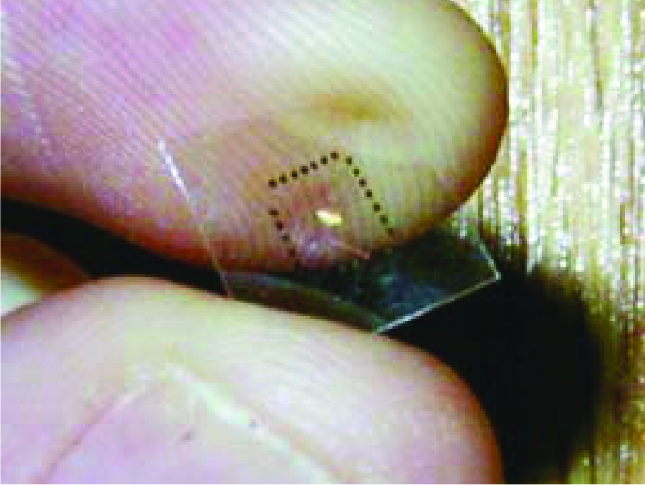
A flexible plastic substrate containing nanowire devices, which don’t degrade when bent.
MCALPINE, FRIEDMAN & LIEBER, HARVARD U.


