Photoelectrons shine a light on dark excitons
DOI: 10.1063/PT.3.4674
When a valence electron jumps across a bandgap to the conduction band, it doesn’t always escape the hole it left behind. In some materials, Coulomb forces are strong enough to hold negatively charged electrons and positively charged holes together in neutral electron–hole pairs known as excitons. The prevalence and dynamics of those quasiparticles affect the electronic and optoelectronic properties of the materials that host them.
Excitons come in two types, bright and dark. A bright exciton forms when a single photon is absorbed. In the case of dark excitons, the electron and hole are connected by an optically forbidden transition, meaning the electron didn’t reach the conduction band through photon absorption alone—it also needed a boost from phonon scattering. Because they lack a signature formation or recombination pathway, dark excitons are difficult to study through the usual optical methods.
Now Julien Madéo and Michael Man, both at the Okinawa Institute of Science and Technology (OIST) in Japan, and their coworkers have turned instead to angle-resolved photoemission spectroscopy (ARPES) for observing dark excitons. 1 Their novel application of the technique detected both bright and dark excitons and monitored the populations over time. Using two different photon energies to create excitons produced the same surprising result: Dark excitons were twice as prevalent as their bright counterparts. The finding shows the importance of dark-exciton dynamics to understanding the optoelectronic properties of exciton-rich materials.
Reduced dimensionality
Although excitonic states exist in all bandgap materials, their natures vary. In bulk semiconductors, for example, the electrons and holes are often so weakly bound that room-temperature thermal fluctuations can break them apart. However, in transition-metal dichalcogenide (TMD) semiconductors, the attraction strengthens when the material’s dimensions are reduced from three to two. 2 (For more about two-dimensional materials, see the article by Pulickel Ajayan, Philip Kim, and Kaustav Banerjee, Physics Today, September 2016, page 38 .) The electrostatic force that binds electrons and holes together is largely shielded in bulk TMDs, but not in monolayers. The tightly bound excitons are more robust, so they play a bigger role in electron dynamics and are easier to study.
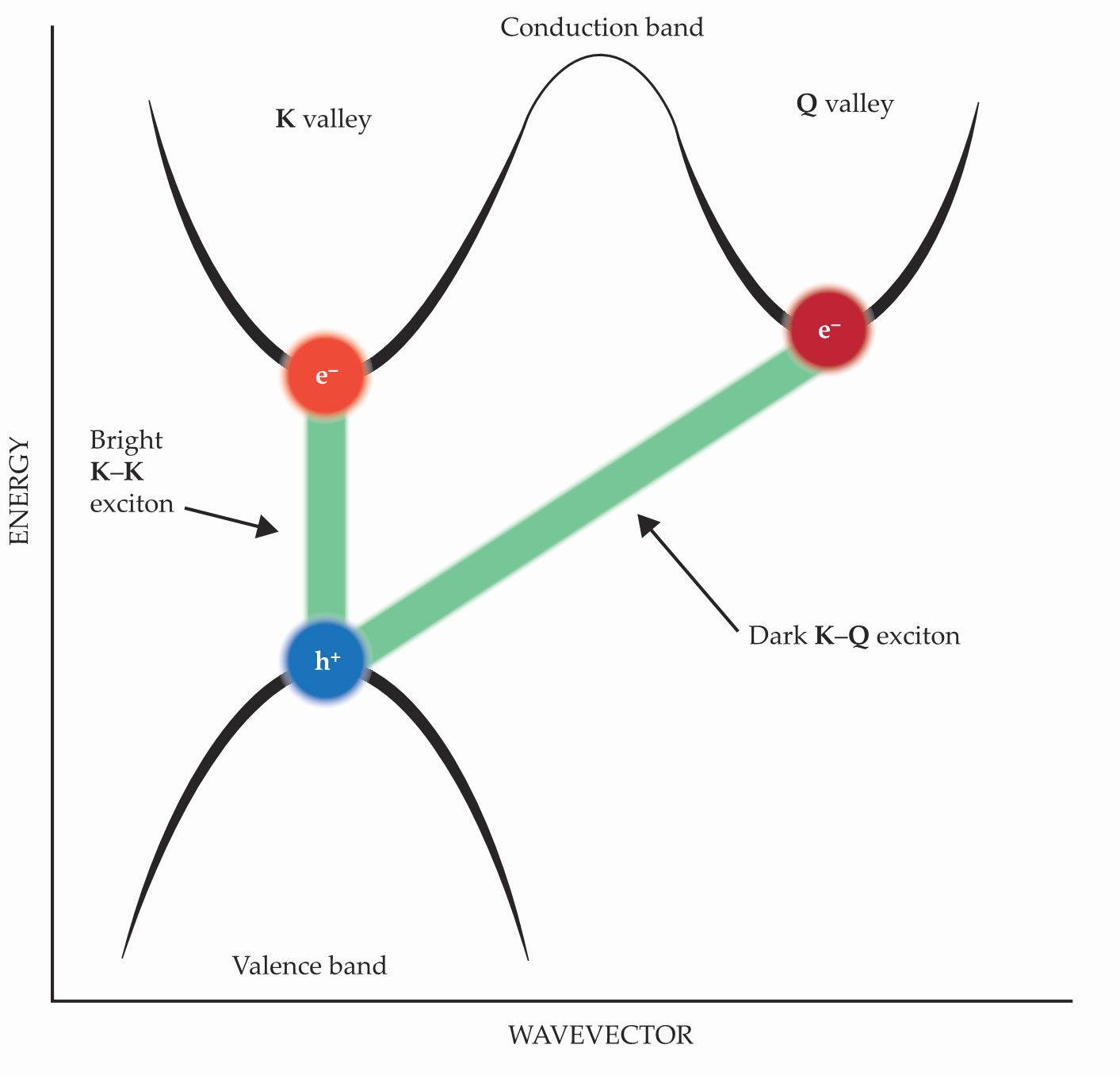
Madéo, Man, and colleagues focused their attention on a particular TMD, tungsten diselenide. Bulk WSe2 has only an indirect bandgap—the peak in its valence band and the lowest point of its conduction band have different momenta—so the gap can’t be traversed using photon absorption alone. But monolayer WSe2 has both a direct and an indirect bandgap, as illustrated in figure
Figure 1.

The electron band structure in monolayer tungsten diselenide has both a valence-band peak and a conduction-band valley at wavevector K. An electron can jump directly across the bandgap by absorbing a single photon to form a bright K–K exciton. However, the WSe2 conduction band has a second energy minimum, at wavevector Q, whose depth is almost identical to that at the K valley. A K–Q exciton is called dark because it can form only if phonon scattering knocks an excited electron into the Q minimum. (Adapted from ref.
The bright excitons created through WSe2’s direct transition make the material photoluminescent and open potential applications in such devices as flexible transistors, photodetectors, and optical switches. 3 And because tightly bound excitons—both bright and dark—form readily in WSe2, their dynamics control the compound’s optoelectronic behavior.
The conduction band of monolayer WSe2 has minima at two wavevectors, K and Q in the usual nomenclature, that correspond to high-symmetry points in the material’s Brillouin zone, the unit cell in momentum space. Valence electrons can be excited into one of those two valleys, which have nearly identical energies but different momenta. The valence band peaks at the K wavevector, so a few-eV photon can push an electron across the bandgap into a K valley to form a K–K exciton. But the photon can’t impart enough momentum to push that electron into the Q valley, which is why K–Q excitons are called “dark.” Something else—typically a phonon—needs to provide an extra kick to make that transition happen.
Photoelectron probes
Optical techniques such as pump–probe and luminescence spectroscopy work fine for studying bright excitons but less well for dark ones. Dark excitons don’t form by the absorption of photons at a particular energy, and their possible routes to recombination—scattering into a bright state, interacting with a lower-lying defect state, or another indirect path—produce ambiguous signals.
ARPES, on the other hand, directly characterizes the electrons in excitons rather than probing their transitions. It’s a go-to technique for exploring electronic structures: Incident photons kick electrons out of a target material and the electrons’ energies and momenta are measured. But experimental challenges have prevented its application to excitons. The experiment must have a source of extreme-UV (XUV) photons to break apart the tightly bound electron–hole pairs and eject photoelectrons, subpicosecond temporal resolution to follow the exciton population’s evolution, and micron-scale spatial resolution to probe tiny samples of high-quality exciton-hosting materials.
“Several leading research groups in the world were thinking of ways to use ARPES-based methods to study excitons over the past decade,” says Keshav Dani, head of the OIST group that led the study. In fact, developing capabilities for temporally and spatially resolved photoemission measurements in novel semiconductor systems was a goal of Dani’s when he founded his group in 2011, the same year OIST opened. Dani credits the young university’s emphasis on interdisciplinary and international collaboration with the group’s success: “The unique institutional and administrative environment is fundamental to the sustained pursuit of creative, high-risk science.” (For more about young research universities, see Physics Today, April 2020, page 22 .)
When Dani began, no one apparatus combined the requisite technologies of XUV-photon sources (XUV-ARPES), subpicosecond temporal resolution (TR-ARPES), and micron-scale spatial resolution (µ-ARPES). And, according to Dani, “It’s not possible to simply combine the standard technologies to do this.” For their new instrument, one of the paper’s lead authors, Man, prepared a µ-ARPES setup using a state-of-the-art electron microscope. Meanwhile, the other lead author, Madéo, developed a high-power, time-resolved XUV-radiation source that could be incorporated into the microscope. By combining those elements with a high-power femtosecond laser, they built an apparatus capable of TR-XUV-µ-ARPES.
Exciton detection
Madéo, Man, and colleagues created excitons in a WSe2 monolayer by resonant excitation—sending in pulses of red photons whose energy, 1.73 eV, was just enough to create an exciton. Pulses of XUV photons then broke the excitons apart. When the excitation and measurement pulses were separated by just a few femtoseconds, the ejected electrons’ momenta peaked at a value consistent with bright excitons. But once the delay between pulses extended to 400 fs, the peak shifted to a momentum value corresponding to a dark exciton (see figure
Figure 2.

Photoelectrons from dark and bright excitons have experimentally indistinguishable energies, but which conduction-band valley they reside in, K or Q, can be determined by their momenta. (a) When bandgap-resonant photons create excitons in monolayer tungsten diselenide, the electrons initially (red dashed line) populate the K valley. After about 0.4 ps (black dashed line), however, many of them have scattered to the Q valley. (b) The steady-state ratio of K- to Q-valley electrons (black) is about 0.5, indicating that the WSe2 monolayer contained nearly twice as many dark excitons as bright ones. The energies of the dark (red) and bright (blue) excitons remain nearly constant throughout. (Adapted from ref.
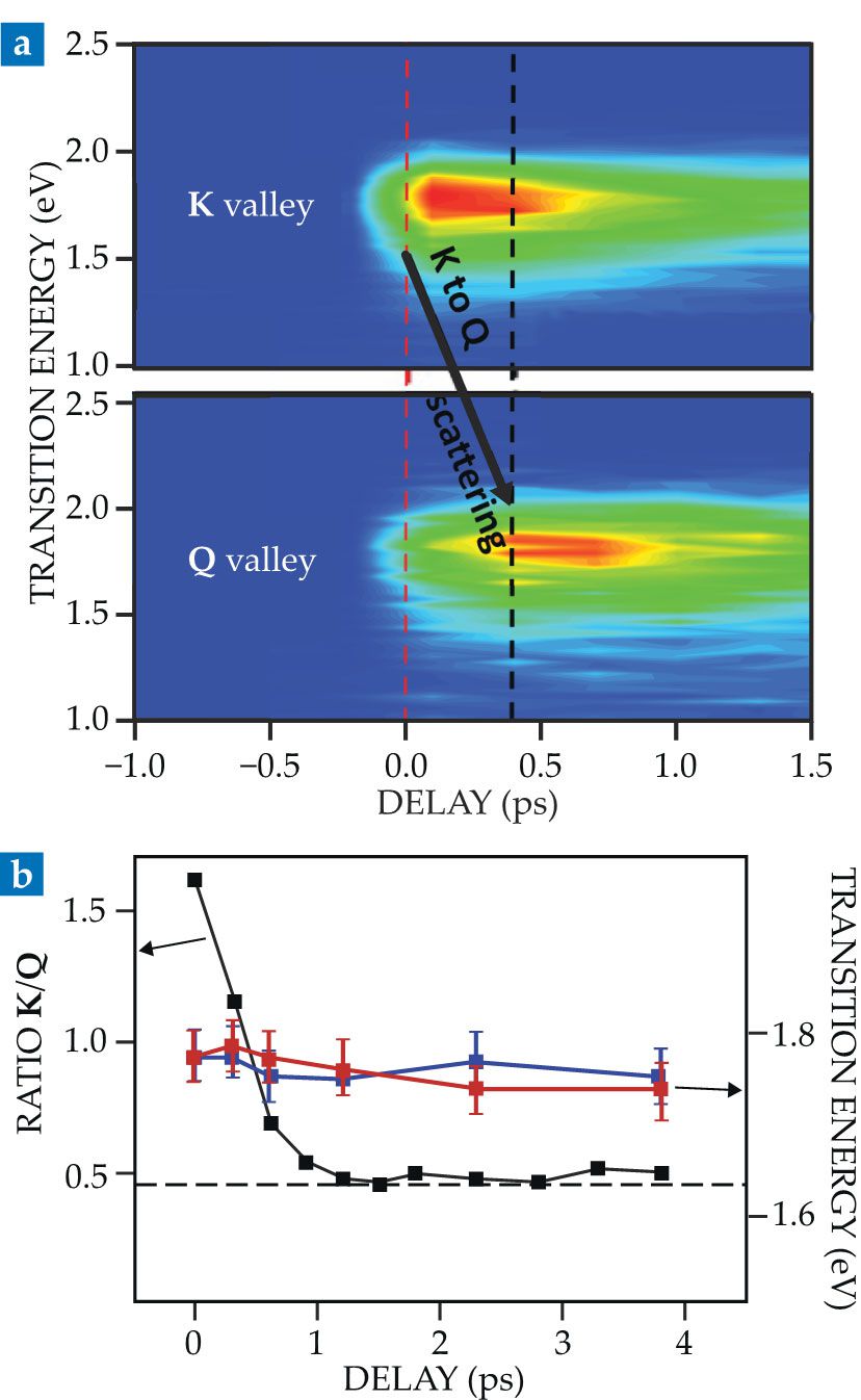
In a second experiment, 2.5 eV photons pushed valence electrons across the bandgap. Some electrons used the additional energy to escape their holes, but after about 300 fs, excitons formed. Unlike what happened in the first experiment, the K–Q excitons formed directly and preferentially, and scattering pushed the population partly into the K valley. After about 1.5 ps, the excitons were again about twice as likely to be dark as bright.
Although the OIST researchers built their own apparatus, their success hinged on contributions from collaborators. The experiments required a high-quality WSe2 monolayer sample, which was provided by Xiaoqin (Elaine) Li’s group at the University of Texas at Austin. And after they made their first successful measurements in spring 2019, Dani and his group reached out to Tony Heinz (Stanford University) and his postdoc Ting Cao (now at the University of Washington) for help interpreting the results. Says Dani, “Discussions with Ting, Tony, and Elaine were invaluable in extracting the right physics out of our data.”
Questions about dark excitons remain, and TR-XUV-µ-ARPES may be able to answer them. Future experiments could, for example, explain why above-gap excitation preferentially produces K–Q excitons, elucidate the role of impurities in exciton scattering, and investigate how dark excitons affect optoelectronic properties.
Lengthier experiments could measure how long dark excitons survive. The current study tracked the quasiparticles for only a few picoseconds, approximately the lifetime of a bright exciton. But a dark exciton’s lifetime is expected to be much longer—perhaps on the order of nanoseconds or more—owing to its strong binding and indirect recombination pathways. 4 That would qualify dark excitons as candidates for use as qubits in future quantum computing devices.
Forbidden transitions involving an electron-spin flip can also produce dark excitons in TMD monolayers, and they’re distinguishable from spin-allowed bright excitons by their energies. Although the current data lack sufficient resolution to separate out those contributions, higher-quality samples should make that possible. Says Dani, “I think the list of future experiments is endless.”
References
1. J. Madéo et al., Science 370, 1199 (2020). https://doi.org/10.1126/science.aba1029
2. G. Wang et al., Rev. Mod. Phys. 90, 021001 (2018). https://doi.org/10.1103/RevModPhys.90.021001
3. K. F. Mak et al., Phys. Rev. Lett. 105, 136805 (2010); https://doi.org/10.1103/PhysRevLett.105.136805
A. Splendiani et al., Nano Lett. 10, 1271 (2010). https://doi.org/10.1021/nl903868w4. Y. Tang, K. F. Mak, J. Shan, Nat. Commun. 10, 4047 (2019). https://doi.org/10.1038/s41467-019-12129-1


