Optically Pumped Silicon Lases in the Near-Infrared
DOI: 10.1063/1.1955466
Silicon has remained the microelectronics industry’s semiconductor of choice for more than a half century. That history makes it a uniquely attractive material for use in photonics: If Si-based devices could manipulate photons within a circuit, the miniaturization of electronics would not suffer as much from problems such as thermal dissipation and increasingly fragile wiring. Engineers could exploit decades-old silicon manufacturing expertise to construct photonic components alongside electronic ones, all on the same chip, to control much speedier trafficking of data among different devices.
In pursuit of that vision, researchers throughout the 1990s developed a suite of silicon components, such as waveguides, multiplexers, optical filters, and photodetectors. A year ago, Mario Paniccia and colleagues from Intel Corp constructed an oxide-gated silicon device that modulates the intensity of an incoming optical beam by converting high-speed electrical signals into optical ones (see Physics Today, April 2004, page 24 ). Developing a silicon laser source has proven more elusive.
Silicon’s band structure accounts for its reluctance to emit light. To appreciate the problem, imagine an excitation in its lattice. The likelihood that the electron–hole pair produced in the crystal recombines to emit a photon depends on where those charge carriers reside in the crystal’s Brillouin zone. The location of the bottom of silicon’s conduction band differs in momentum space from the top of its valence band. That asymmetry means that electrons pumped to the conduction band are more likely to roam around for a long time before re-combining with the holes across the “indirect” bandgap. Indeed, the radiative lifetime of electron–hole pairs in silicon is long, typically milliseconds. And when the charge carriers do recombine, they’re far more likely to produce a quantized lattice vibration—a phonon—than emit a photon.
To overcome the radiative recombination inefficiency, researchers over the years have adopted a number of strategies, mostly to spatially confine the charge carriers; examples include using silicon nanocrystals, quantum dots, and even strained material that modifies the band structure. Four years ago, UCLA’s Bahram Jalali took a different tack to coax light from silicon by using its nonlinear Raman gain coefficient. That approach has paid off: His group and Paniccia’s Intel team have now separately demonstrated lasing from silicon.
Light scattering
Raman amplifiers are not new. Roger Stolen and Erich Ippen had measured the nonlinear Raman gain from glass (SiO2) fiber in 1973. 1 Photons from a pump laser incident on a solid scatter off lattice phonons, an interaction that prompts the reemission of light at a lower energy together with a phonon. A small amplification of the scattered light accompanies the wavelength conversion: The two optical fields—the initial pump wave and the signal, or Stokes, wave created by the phonon scattering—interact to produce a force that drives the vibrations in the lattice at the difference frequency. The effect is to transfer power from the optical pump to the signal wave.
Although a weak effect, the nonlinear gain adds up if given enough room. Stolen and Ippen’s work with silica (SiO2) set the stage for using kilometer-length glass fibers as broadband amplifiers of telecommunication signals and as tunable oscillators. Commercial silica amplifiers help sustain most long-distance telephone calls made today. Because silica is amorphous, the atomic vibrations that lead to its Raman effect are spread into broad bands; as a result, silica amplifiers have enormous output bandwidth, at the expense of having low gain.
In contrast, crystalline silicon scatters light into a single optical mode. That makes its Raman gain nearly 104 times as much as in silica, provided the light intensity is high enough to drive the process. Thanks to its high purity and high index of refraction, silicon also forms the heart of waveguides that can preserve those high intensities over long distances: A ridged layer of Si, clad above and below by SiO2 (which has a lower index of refraction), tightly confines the beam. This optical confinement effect, coupled with silicon’s Raman gain, gave Jalali confidence that an amplifier could be fashioned into a compact device.
Over the last couple of years, a number of other researchers joined the effort, much of which led to reducing light losses and noise. In October 2004, shortly after building a Raman amplifier, Jalali and his postdoc Ozdal Boyraz yoked the amplifier to a cavity resonator and first demonstrated a silicon Raman laser. 2
The UCLA device used a pulsed near-IR pump laser to drive a Si-crystal waveguide attached at both ends of an 8-meter fiber that served as a ring cavity resonator to provide positive feedback. To reach Raman lasing, Jalali increased the pump power until the optical gain just exceeded the net loss on each round trip through the crystal; the telltale sign was a sudden increase in the coherent emission spectrum at a frequency downshifted by 15.6 THz, the frequency of silicon’s optical phonons.
Silicon is transparent in the near-IR. But increasing the pump intensity also increases the probability that the lattice will absorb two photons at once. Added together, the photon energies excite silicon electrons above its bandgap, creating free carriers in the waveguide. Those carriers can absorb enough signal light to kill the amplification process. The problem limited the UCLA laser to pulsed emission from a pulsed source; short pulse widths spaced by a period longer than the free-carrier lifetimes prevent undesired carrier buildup.
Working in parallel with Jalali’s group, Paniccia and his Intel colleagues developed their own all-Si pulsed laser in January of this year, and more recently improved on the design to largely solve the two-photon absorption problem (see figure 1 on previous page). 3 The group added partially reflective dielectric mirrors to the ends of an S-shaped waveguide and made the device self-contained on the chip without the need for an external fiber; they also doped the edges of the intrinsic-silicon waveguide.

Figure 1. A silicon Raman laser consists of a “rib” waveguide made from crystalline silicon enclosed in a sheath of silica (SiO2) cladding and pumped by a separate laser. The figure shows on-edge (left) and lateral (middle) views of the waveguide. Partially reflective mirrors form a resonator cavity tuned to the frequency of the Raman emission. The pump light (blue) exploits the nonlinear Raman effect, provided the pump is intense enough to couple to the material’s optical phonons and emit stimulated, coherent scattered waves back through the waveguide. But if too intense, the pump light also excites electrons and holes into the lattice, which kills the Raman gain. An electric field applied across n- and p-doped regions sweeps them away. At far right, eight Si-based Raman lasers sit on a 16 mm by 16 mm chip.
(Adapted from ref. 3; courtesy of Intel Corp.)
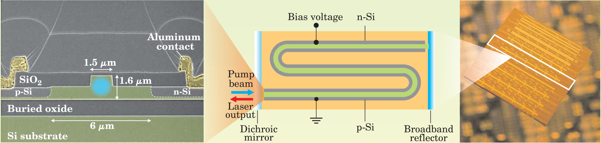
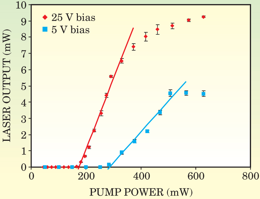
Voltage applied to the n-doped silicon relative to the p-doped region creates an electric field that sweeps away most of the electrons and holes formed by the high pump-beam intensity. The configuration allowed the team to pump the crystal continuously from a diode laser at 1.55 µm without saturating the silicon with charge carriers. And it produced a similar continuous-wave emission at a Stokes wavelength of 1.69 µm. Figure 2 illustrates how biasing the diode influences the threshold for stimulated Raman scattering.

Figure 2. Applying a voltage between the p- and n-doped regions that straddle the silicon waveguide shortens the free-carrier lifetimes enough to sharply reduce the Raman laser turn-on power and improve the laser’s efficiency. But it doesn’t entirely eliminate the free carriers, if the saturation in output power as pump intensity grows is any indication.
(Adapted from ref. 3.)
Toward practical devices
Paniccia argues that optimizing the system could reduce carrier lifetimes to less than the roughly 1 ns his current device achieves, increase the output power, and lower the lasing threshold still further. But “what’s surprising is, it’s already a pretty good laser,” he says. Threshold powers of a few hundred milliwatts focused into the silicon waveguide generate optical intensities as high as 25 MW/cm2 and output powers of about 8 mW. On the other hand, argues the University of Rochester’s Philippe Fauchet, the devices will always be dependent on another primary light source, the offchip pump. “There’s a big difference between Raman lasers and injection lasers,” which work by electrical pumping of electrons and holes from a pn junction. Still, a Si-based injection laser may be within reach. The last few years have seen efforts to modify silicon’s band structure to make electron–hole recombination more “direct.” There’s even the possibility of exploiting inter-subband transitions rather than band-to-band ones, Fauchet adds.
From the perspective of optical pumping, Caltech’s Kerry Vahala points out that “a wider material palette beyond silicon or silicon-engineered materials is possible.” Using the ultra-low optical loss and tiny mode volumes that toroidal micro-cavities provide, his group has built continuous-wave Raman lasers based on silica. 4
If the primary light source is destined to remain off-chip, why bother using silicon lasers? In the near-IR spectrum widely used in telecommunications, a variety of semiconductor lasers would suffice. But Jalali doesn’t see the silicon laser as a replacement for traditional lasers. Attaching a diode to the waveguide can electrically modulate the continuous signal in a way analogous to Intel’s approach of sweeping the waveguide clean of electrons and holes. 5 Injecting free carriers intermittently kills the signal, an effect that distinguishes silicon lasers from garden-variety Raman devices.
Moreover, Jalali envisions using a silicon laser as a broadly tunable device that extends the wavelength of light by the Stokes wavelength at each stage—eventually into regimes where ordinary semiconductor laser sources cannot reach. At mid-IR wavelengths between 2 and 10 µm, for instance, biochemical detection, laser medicine, free-space optical communication, and even counterterrorism—using silicon lasers to jam the heat-seeking sensors of offensive missiles, say—come to mind as potential applications.
Beyond 2.2 µm, two-phonon absorption energies fall below silicon’s bandgap. At those wavelengths, where few other sources exist, the laser’s biggest problem is solved.
References
1. R. H. Stolen, E. P. Ippen, Appl. Phys. Lett. 22, 276 (1973) https://doi.org/10.1063/1.1654637 .
2. O. Boyraz, B. Jalali, Opt. Express 12, 5269 (2004) https://doi.org/10.1364/OPEX.12.005269 .
3. H. Rong et al., Nature 433, 725 (2005) https://doi.org/10.1038/nature03346 .
4. T. J. Kippenberg et al., Opt. Lett. 29, 1224 (2004) https://doi.org/10.1364/OL.29.001224 .
5. O. Boyraz, B. Jalali, Opt. Express 13, 796 (2005) https://doi.org/10.1364/OPEX.13.000796 .


