Nanowire solar cells made efficient
DOI: 10.1063/PT.3.1904
At first glance, an array of nanowires makes for a lousy solar cell. Their surface-to-volume ratio is huge. So when an absorbed photon produces an electron–hole pair, the charges may separate only briefly (typically driven by a p–n junction fabricated within the wire) before becoming trapped at one of the numerous defects that often reside at the surface. There, the charge carriers are more likely to recombine and thus give up their electrical energy before it can be harnassed in a circuit.
Still, a nanowire architecture has natural appeal: Scarce but highly absorptive semiconductors can be configured into photovoltaics that use far less material than those made from conventional thin films. Some III–V semiconductors, for example, have absorption coefficients a thousand times greater than silicon. But none of the earlier nanowire devices based on them have surpassed power-conversion efficiencies of 3–5%. That’s well below the roughly 20% that can be achieved using conventional planar Si films (see the article by George Crabtree and Nathan Lewis in Physics Today, March 2007, page 37 ).
Researchers led by Magnus Borgström (Lund University in Sweden) have now shown that a judicious choice of material and refinements to its growth can dramatically improve the efficiency of a nanowire array. 1 They used the III–V semiconductor indium phosphide because it tends to exhibit slower electron–hole surface recombination; surface states that form from dangling bonds and oxides on untreated InP simply don’t trap carriers as voraciously as do, for instance, surface defects in Si or gallium arsenide.
Through modeling, Borgström and coworkers identified two key design parameters that influence device performance: the InP nanowire diameter and the length of its topmost n-doped segment, as illustrated in the figure below. The model showed that a diameter of about 200 nm would optimize the wires’ absorption across the Sun’s broad spectrum. And indeed, experimental tests confirmed that absorption increased with increasing diameter until it saturated around 180 nm.

This array of indium phosphide nanowires, pictured in scanning electron micrographs (a) from the top and on angle, is a small fraction of the full array of 4 million nanowires that compose a solar cell epitaxially grown on a 1-mm2 InP substrate. (b) The layered p-doped, intrinsic, and n-doped segments, viewed here from the side, are enveloped by silicon dioxide (blue) to insulate individual wires from each other and by a transparent conducting oxide (red) that connects the wires to electrodes. (Adapted from ref.
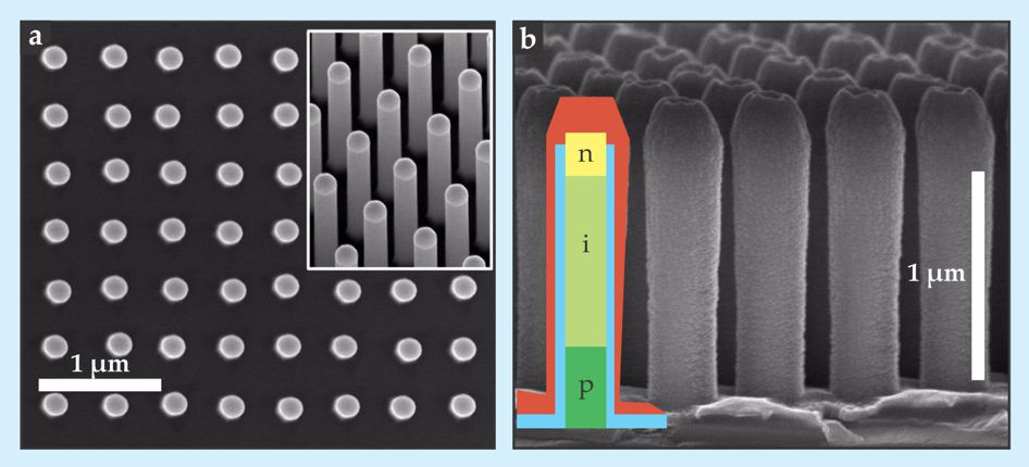
To optimize conduction properties, the researchers used a 60-year-old epitaxial method, metal organic chemical vapor deposition, to synthesize the InP nanowires from the vapor phase. Specifically, they grew them as vertically stacked layers of p-doped, undoped (intrinsic), and n-doped material, an approach that enabled fine control over the length of each region. The doped regions are needed to separate the charges, but the shorter they are, the slower the electron–hole pair recombination. Because high-energy photons produce the most charge carriers near the top of each nanowire, the reduction of doped material there significantly increased current densities.
In addition, as the wires were growing, the team etched them in acid, which kept them ramrod straight and impeded any radial growth that could effectively short-circuit parts of the p-i-n junctions.
As proof of concept, the researchers built an InP solar cell, partially shown in the figure, composed of 4 million nanowires 180 nm in diameter and 1.5 µm tall, arranged in a square array in which the wires are spaced about 500 nm apart. The device converted about 14% of the incoming light into electric power—nearly triple what had been produced in earlier InP arrays and a new record for nanowire solar cells. The current density delivered by the array is nearly as great as that produced by conventional InP thin-film cells, despite the nanowires’ surface packing fraction of just 12%.
The enhanced optical absorption of the device arises from the ability of the nanowires, with diameters below the wavelength of visible light, to confine incoming rays into guided electromagnetic modes. Like miniature antennae, the nanowires concentrate incoming electromagnetic waves. Important to their success is that the spacing between wires is well matched to the wavelength at which the solar intensity peaks.
“Although the new design’s efficiency remains below that of silicon cells, it’s an impressive achievement that will bring validation to the nanowire community—and probably draw more people into the field,” comments Stanford University’s Michael McGehee. “But it’s certainly not high enough to launch a product,” he cautions.
There is a straightforward path to higher performance, at least in principle. One can break the Shockley–Queisser limit, which establishes the maximum conversion efficiency of a solar cell having a single bandgap, by chemically altering the nanowires’ growth to emplace multiple materials on top of each other. The different constituent materials absorb different parts of the solar spectrum. That’s on the to-do list, Borgström says, noting that it’s much easier to pull off in a nanowire architecture than in thin films, which can suffer more from lattice strain at the interface between materials.
“When we reach 30% efficiency, then we’ll have a commercially interesting product,” he says. Interesting indeed: Solar cells are already a $100 billion industry that is growing at more than 30% a year.
References
1. J. Wallentin et al., Science (in press). http://dx.doi.org/10.1126/science.1230969 https://doi.org/10.1126/science.1230969


