Molecular Electronics
DOI: 10.1063/1.1583533
Imagine molecular gears that oscillate against each other as they are stimulated by the addition or removal of a single electron, 1 or a domino-like arrangement of molecules in which a small perturbation on one end initiates a molecular-mechanical cascade that ripples through the whole assembly in a predetermined fashion. 2 Imagine a wire in which the presence or absence of a single atom dominates the electrical conductivity, 3 or in which a biomolecular recognition process is used to open up new conductivity pathways. 4 These descriptions are respectively those of a molecular-mechanical switch that forms the basis of a random access memory circuit, a molecular-based three-input mechanical Boolean sorter, a single-molecule electrically or magnetically gated switch, and a single-stranded DNA wire that is “turned on” by hybridization of the DNA into the double-stranded form. These molecular systems, and a host of other equally diverse chemical species, are principal actors in the rapidly emerging field of molecular electronics.
Molecules have not historically played a prominent role in electronic devices. Ten years ago, chemical applications were limited to the use of small molecules such as silanes (Si x H y ) and germanes (Ge x H y ) as thin-film precursors or as the components of etching processes, resist precursors, packaging materials, and the like. Engineered inorganic insulators, semiconductors, and metals were the heart of the industry, and the fundamental knowledge that gave birth to the integrated circuit was appropriately credited back to the fundamental solid-state physics that was largely developed in the mid-20th century.
Over the past decade, the picture has not changed much. Conducting polymers have emerged as a real, albeit still minor, technology. However, over the next 10–20 years, molecules may be increasingly viewed not just as the starting points for bulk electronic materials, but as the active device components within electronic circuitry (see, for instance, figure 1). Although this possibility is hardly a foregone conclusion, a number of fundamental issues favor the development of a true molecular-based electronics.

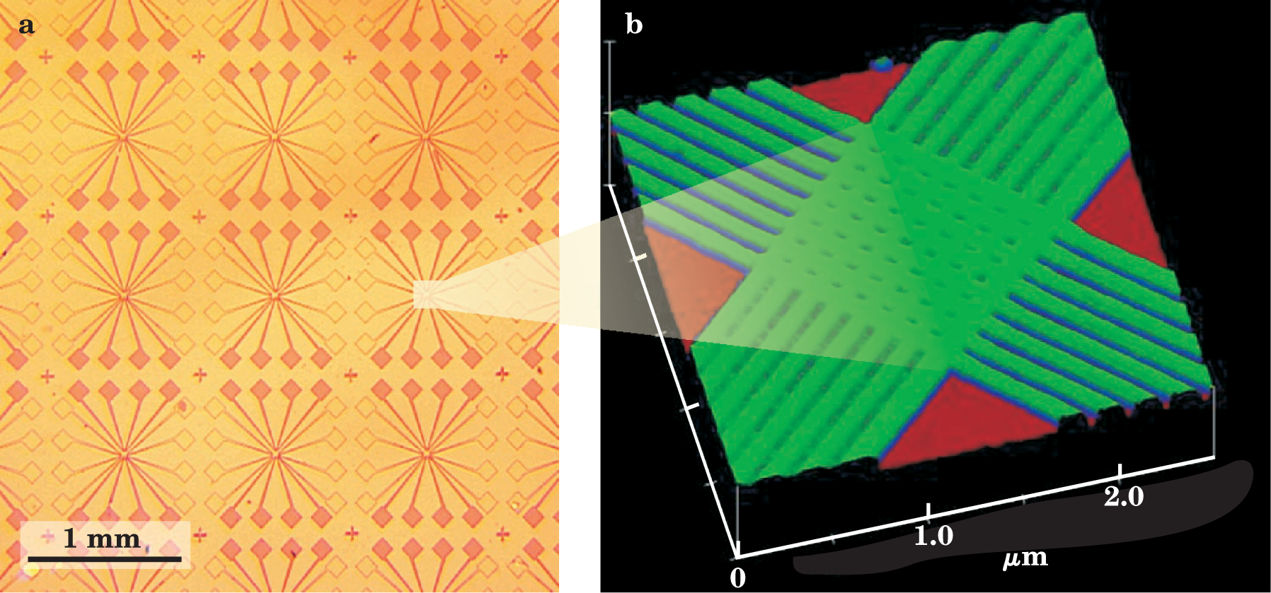
Figure 1. Molecular electronics devices. (a) This optical micrograph shows a collection of 64-junction molecular circuits, fabricated by a combination of soft-imprinting techniques for the wires and chemical assembly for the molecules at the wire intersections. (b) An atomic force micrograph of one of the circuits, which could be used either as a random access memory or as a combination logic and memory circuit. The molecules used in this circuit are bistable [2]rotaxanes.
(Adapted from Y. Chen et al., ref. 13. Courtesy of Stan Williams, Hewlett-Packard Co.)
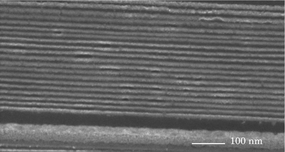
Consider the lattice of nanowires 5 in the electron micrograph of figure 2. Each wire is 5 nm in diameter, and the lattice constant is 15 nm. At a typical doping level of 1018 atoms of boron or arsenic per cubic centimeter, similar 5-nm diameter, micron-long segments of silicon wires would have 15–20 dopant atoms, and a junction of two crossed wires would contain, on average, approximately 0.1 dopant atom. Consequently, field-effect transistors fabricated at these wiring densities might exhibit non-statistical, and perhaps unpredictable, behavior. Other concerns, such as the gate oxide thickness, power consumption (just from leakage currents through the gate oxide), and fabrication costs, also highlight the difficulty of scaling standard electronics materials to molecular dimensions. 6 At device areas of a few tens of square nanometers, molecules have an inherent attractiveness because of their size, because they represent the ultimate in terms of atomic control over physical properties, and because of the diversity of properties—such as switching, dynamic organization, and recognition—that can be achieved through such control.

Figure 2. Array of nanowires, each approximately 5 nm in diameter. The lattice constant is about 15 nm. Certain materials parameters important to solid-state devices, such as the average density of dopant atoms, no longer hold meaning at these nanoscale dimensions. At this size scale, however, chemical control over molecular properties is highly developed.
Although molecular electronics has been the subject of research for some time, over the past few years a number of synthetic and quantum chemists, physicists, engineers, and other researchers have sharply increased the ranks of this field. Several new molecular-electronic systems, analytical tools, and device architectures have been introduced and explored. As a result, the basic science on which a molecular electronics technology would be built is now unfolding, and the science and applications that are emerging are tremendously exciting. For example, current research is using molecules in such electronics applications as interconnects, switches, rectifiers, transistors, nonlinear components, dielectrics, photovoltaics, and memories. Excellent reviews of this field are available. 7 In this article, we focus on the current state of the art in one area of molecular electronics, with an emphasis on the relationship between molecular structure and electrical conductance and on the use of molecules for computational applications. The essential science in these areas reflects the broader field of molecular electronics, and although certain fundamental challenges have been faced, many others must still be overcome.
Why molecular electronics?
Essentially all electronic processes in nature, from photosynthesis to signal transduction, occur in molecular structures. For electronics applications, molecular structures have four major advantages:
-
▸ Size. The size scale of molecules is between 1 and 100 nm, a scale that permits functional nanostructures with accompanying advantages in cost, efficiency, and power dissipation.
-
▸ Assembly and recognition. One can exploit specific intermolecular interactions to form structures by nano-scale self-assembly. Molecular recognition can be used to modify electronic behavior, providing both switching and sensing capabilities on the single-molecule scale.
-
▸ Dynamical stereochemistry. Many molecules have multiple distinct stable geometric structures or isomers (an example is the rotaxane molecule in figure
3(d) , in which a rectangular slider has two stable binding sites along a linear track). Such geometric isomers can have distinct optical and electronic properties. For example, the retinal molecule switches between two stable structures, a process that transduces light into a chemoelectrical pulse and allows vision. -
▸ Synthetic tailorability By choice of composition and geometry, one can extensively vary a molecule’s transport, binding, optical, and structural properties. The tools of molecular synthesis are highly developed.
Molecules have disadvantages, though, such as instability at high temperatures. But overall, the four advantages render molecules ideal for electronics applications, as Richard Feynman noted in his famous 1959 speech, “There is Plenty of Room at the Bottom.”
Mechanisms of molecular charge transport
The synthesis and characterization of molecules are endeavors typically conducted in solution. Decades of research have given chemists intuitive models that serve as a guide for using synthetic control to design physical properties into a molecule. A key challenge in molecular electronics is to translate that solution-phase intuition into a solid-state device setting. Certain molecular structures have emerged as models for relating intramolecular electron transfer rates in solution to solid-state molecular junction conductance.
A picture of electron transport through molecular devices is emerging, and it couldn’t be more different from what is observed for more traditional conductors. Disregard, for the moment, the details of the electrical contact. In a semiconductor or metal wire, charge transport is ohmic: For a given wire diameter, longer wires have proportionately higher resistance. Such a picture is usually wrong for molecules because of the localized nature of most molecular electronic states.
Consider the energy diagrams of figure 3, in which four types of molecular-electronic junctions are represented, with examples of molecular structures. In figure

Figure 3. Examples of molecular transport junctions. The top panels depict molecules with various localized, low-energy molecular orbitals (colored dots) bridging two electrodes L (left) and R (right). In the middle panels, the black lines are unperturbed electronic energy levels; the red lines indicate energy levels under an applied field. The bottom panels depict representative molecular structures. (a) A linear chain, or alkane. (b) A donor-bridge-acceptor (DBA) molecule, with a distance / between the donor and acceptor and an energy difference E B between the acceptor and the bridge. (c) A molecular quantum dot system. The transport is dominated by the single metal atom contained in the molecule. (d) An organic molecule with several different functional groups (distinct subunits) bridging the electrode gap. The molecule shown is a [2]rotaxane, which displays a diverse set of localized molecular sites along the extended chain. Two of those sites (red and green) provide positions on which the sliding rectangular unit (blue) can stably sit. A second example of a complex molecule bridging the electrodes might be a short DNA chain.
((c) Adapted from ref. 3.)
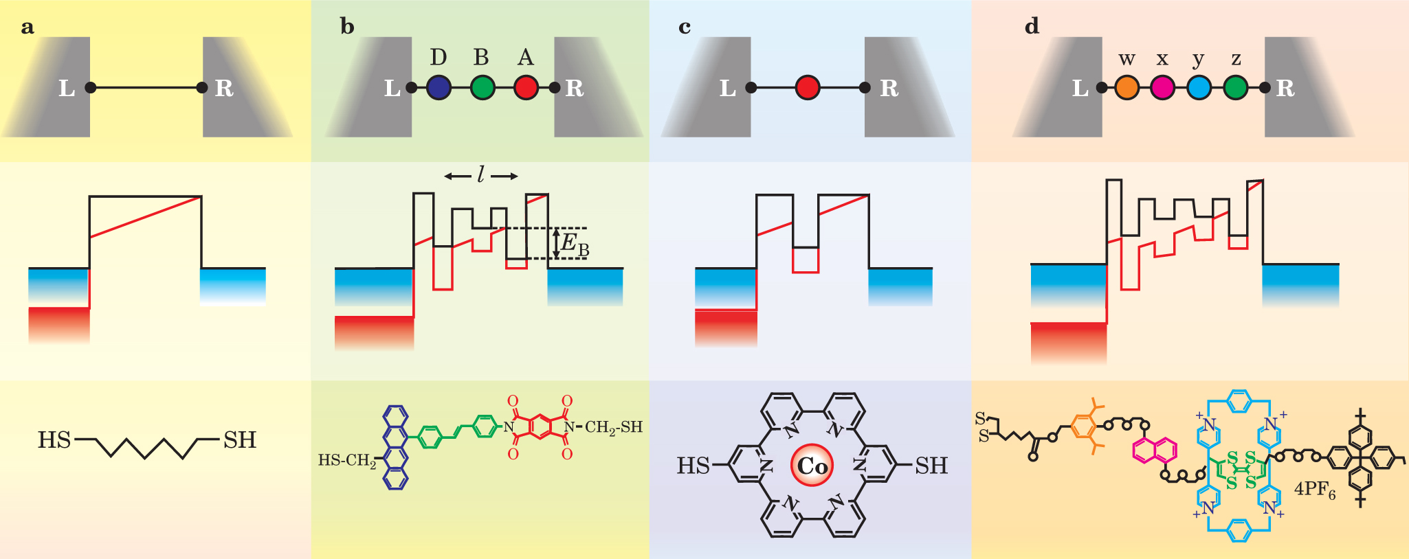
The possible mechanisms for electron transport are much richer for the electron donor-bridge-electron acceptor (DBA) molecular junction of figure
DBA junctions illustrate some of the beauty and richness of molecular electronics. From a chemist’s perspective, the diversity of conduction mechanisms represents an opportunity to manipulate the electrical properties of junctions through synthetic modification. The observed conduction in DBA molecular junctions usually differs radically from that in traditional ohmic wires and can more closely resemble coherent transport in mesoscopic structures. Key factors include a dependence on the rates of intramolecular electron transfer between the donor and acceptor sites. This dependence can be exploited: The donor and acceptor components could be designed to differ energetically from one another (as in figure
The competition between charge transport mechanisms through a DBA molecule can also be affected by the bridge. Shorter bridges produce larger amounts of wave-function overlap between the donor and acceptor molecular orbitals. For a short bridge (5–10 Å), the superexchange mechanism will almost always dominate. For sufficiently long bridges, the hopping mechanism will almost always dominate. The molecular structure of the bridge can be synthetically varied to control the relative importance of the two mechanisms. For example, in a bridge containing conjugated double bonds, low-lying unoccupied electronic states within the bridge will decrease in energy with increasing bridge length (E B of figure
Certain molecules will isomerize—that is, change shape—upon receiving a charge or being placed in a strong field, and in many cases, such transformations can be highly controlled. Different molecular isomers are characterized by different energies and possibly by different relative rates for the hopping and superexchange transport mechanisms. Driven molecular isomerization therefore presents opportunities for designing switches and other active device elements. 1
Molecular quantum dots (figure
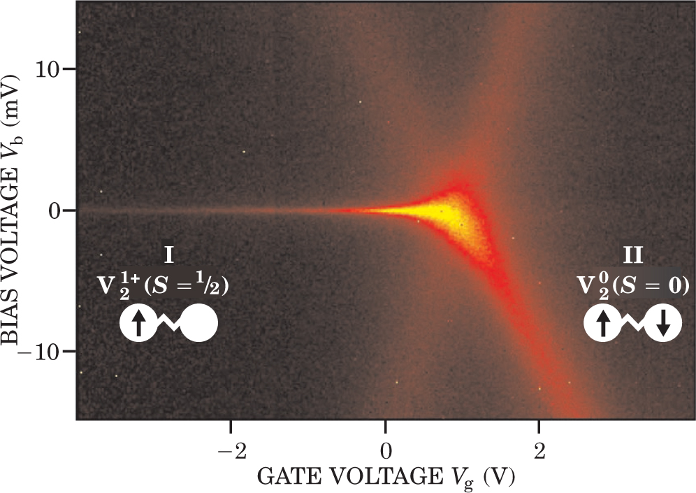
Two recent papers reported on a unique quantum effect known as a Kondo resonance (see figure 4) in organic molecules containing paramagnetic metal atoms. 3 That this resonance was designed by chemical synthesis into two different molecules, and was observed in single-molecule transport measurements, represents a spectacular success for molecular electronics.

Figure 4. Observations of Kondo resonances are a triumph of molecular synthesis and junction fabrication. Plotted here is the differential conductance obtained as a function of bias voltage V b and gate voltage V g of a single divanadium molecule, connected to two electrodes and coupled to a gate electrode. The two vanadium atoms are separated by a short organic bridge (denoted as the two white spheres separated by a jagged line). Black indicates low conductance; yellow is high conductance. The two conductance-gap regions, labeled I and II, are bounded by two peaks that slope linearly with V g. The peaks cross for V g around 1 V, at which point the conductance gap vanishes. The sharp zero-bias peak in region I is a Kondo resonance, which results from the formation of a bound state arising from a quantum mechanical exchange interaction between an electron on the divanadium and the electrode. The resonance appears only when the electronic state of the divanadium has non-zero spin S.
Current in an elastic molecular wire junction
The simplest molecular wire structure comprises a molecule bonded (perhaps by a sulfur-gold, carbon-carbon or silicon-carbon bond) through a single atom to electrodes at the two molecular termini. Rolf Landauer stressed that charge can move through such a structure by elastic scattering—in other words, “conductance is scattering.”
Mathematically, the Landauer formula is
Here g is the conductance, e is the electron charge, h is Planck’s constant, and Tij is the scattering probability from incoming channel i to outgoing channel j. If there is one open channel without scattering, g = 2e 2/h = (12.8 kω)−1, the quantum of conductance.
If one generalizes the Landauer approach to a molecular wire at small voltages, 7 the conductance can be written as
Here G M is the Green’s function that characterizes electron scattering between ends of the molecule. The spectral densities ΓR and ΓL describe the effective mixing strength between molecule and electrode at the left and right ends, respectively. Electronic structure theory permits actual calculation of g, once the geometries are known. 7
Electrode effects
The molecule–electrode interface is a critically important component of a molecular junction: It may limit current flow or completely modify the measured electrical response of the junction. Most experimental platforms for constructing molecular-electronic devices are based on practical considerations. This pragmatic approach is, in many ways, the boon and the bane of the field. For example, the sulfur-gold bond is a terrific chemical handle for forming self-assembled, robust organic monolayers on metal surfaces. Other methods, such as using a scanning probe tip to contact the molecule, are frequently employed, in part because they avoid processing steps that can damage or unpredictably modify the molecular component. Ideally, the choice of electrode materials would be based not on the ease of fabrication or measurement, but rather on first-principles considerations of molecule-electrode interactions. However, the current state of the art for the theory of molecule-electrode interfaces is primitive.
Poor covalent bonding usually exists between the molecule and electrode. Consequently, at zero applied bias some charge must flow between molecule and electrode to equilibrate the chemical potential across the junction. That flow can cause partial charging of the molecule, and local charge buildup gives Schottky-like barriers to charge flow across the interface. Such barriers, which can partially or fully mask the electronic signature of the molecule, increase for larger electronegativity differences. For this reason—and others, including stability, reproducibility, and generality—chemical bonds such as carbon-carbon or silicon-carbon will likely be preferred over sulfur-gold linkages at the interfaces.
Very little theory exists that can adequately predict how the energy levels of the molecular orbitals will align with the Fermi energy of the electrode. Small changes in the energy levels can dramatically affect junction conductance, so understanding how the interface energy levels correlate is critical and demands both theoretical and experimental study. A related consideration involves how the chemical nature of the molecule-electrode interface affects the rest of the molecule. The zero-bias coherent conductance of a molecular junction may be described as a product of functions that describe the molecule’s electronic structure and the molecule-electrode interfaces (see
Conductance through DNA
Figure
DNA oligomers represent perhaps the best-studied experimental example of this category. In addition to its biological importance and its use as a synthetic component of molecular nanostructures, the DNA molecule is of interest as a charge transfer species. 4 Here the relationship between intramolecular electron transfer rates in solution and solid-state molecular junction transport becomes crucial to our understanding of transport processes. Connections to electrodes are also of great importance.
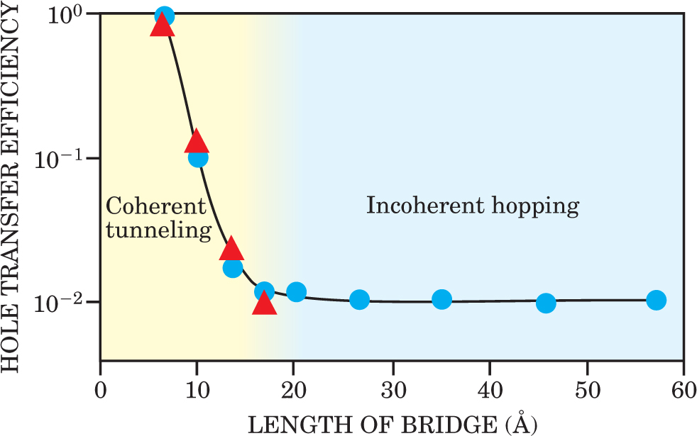
Intramolecular electron transfer rates in DNA have been extensively investigated in solution, and it is now becoming clear that the underlying processes exhibit a large mechanistic diversity. In general, for very short-distance motion (over a few base pairs), coherent tunneling can occur. For transfer over more than six or seven base pairs, inelastic hopping has been strongly suggested. The fundamental motion of electrons or holes from one site to another very broadly follows the standard model developed by Rudy Marcus, Noel Hush, and Joshua Jortner for charge transfer rates. The model assumes that for a charge tunneling from a donor to an acceptor site, the tunneling parameters—the height and width of the tunnel barrier—are modulated by interactions with a bath of harmonic oscillators that account for the chemical environment. An exponential decay in the conductance with increasing distance has been seen directly in DNA molecules folded into hairpin shapes, and the transition to incoherent hopping has been seen in measurements of the efficiency with which holes are transferred along the molecule. The rich mechanistic palette observed for DNA charge transfer is becoming well understood due to elegant experiments and theory (see, for instance, figure 5). 4,10 Indeed, the early suggestions that, because of its broad range of mechanistic possibilities, DNA might act as a paradigm for electron transfer generally seem to be correct.

Figure 5. DNA shows a competition between different charge transport mechanisms. Plotted here are the experimental (triangles and circles) and theoretical (solid line) results for the relative rate of hole transfer between guanine-cytosine (GC) base pairs on DNA oligomers. The theoretical model incorporates both tunneling for nearest neighbor GC pairs and hopping between GC pairs separated by a bridge of several adenosine-thymine pairs, which have higher energy. Coherent tunneling dominates for short distances, and shows a characteristic exponential decay. Incoherent hopping dominates over long distances.
(Adapted from ref. 10.)
Electrical transport in DNA molecular junctions is much messier—as should be true for any molecular junction of the type represented in figure
Most probably, transport in DNA junctions will show that the molecule (or at least naturally occurring DNA) is essentially a wide-bandgap semiconductor characterized by localized hole hopping between the low-energy guanine-cytosine (GC) pairs (G yields the most stable positive ion). Because the bandgap is large, DNA appears uncolored and long-range coherent charge motion is improbable. Significant effects should arise from various other processes, such as polaron-type hopping, in which charge motion is accompanied by molecular distortion; Anderson-type charge localization, caused by the difference in energy between electrons localized on GC and adenosine-thymine (AT) pairs; structural reorganization; counter-ion motion; and solvent dynamics. The available data are, more or less, consistent with the suggestion by Cees Dekker and his collaborators that DNA is a wide-bandgap semiconductor 11 that can exhibit activated transport for relatively short distances (less than 10 nm or so) but effectively behaves as an insulator at distances exceeding 20 nm. The complexity and richness of DNA junction behavior typify the challenge that the molecular electronics community faces in predicting and understanding transport in molecular junctions.
Molecular electronics circuits
The power of chemical synthesis to design specific and perhaps even useful device behaviors is rapidly being realized. The ensuing question, what sorts of circuit architectures can best take advantage of molecular electronics, is now receiving quite a bit of attention both from computer scientists (who have published largely in the patent literature) and from experimentalists; progress toward identifying and constructing working molecular electronics circuitry has advanced quickly. The proposed circuit architectures have attempted to deal with five key issues: scalability to near molecular dimensions; tolerance of manufacturing defects; introduction of nontraditional fabrication methods, such as chemically directed assembly; bridging between device densities potentially achievable at the molecular scale and those associated with standard lithography; and fabrication simplicity.
The dominant circuit structure that has arisen from those considerations is the crossbar,
12
which is essentially an expanded ticktacktoe board formed from wires and having individual molecular or molecular-scale devices sandwiched within the junctions. The crossbar is an intrinsically versatile circuit and is tolerant of manufacturing defects. Both memory and logic circuits have been demonstrated from molecular electronics and nanowire cross-bars.
1,13
A rapidly developing area of architectural research involves stitching together a patchwork quilt of different types of crossbars with the goal of configuring an efficient computational platform.
14
Crossbars and demultiplexers
One of the most attractive architectures for designing molecular-electronics circuits for computational applications and interfacing them to the macroscopic world is the crossbar. The general concept is shown on the left, where a sort of patchwork quilt of logic, memory, and signal routing circuits is laid out. The simplest of these circuits—and one that has been experimentally demonstrated—is a memory circuit.
The memory, shown on the right, consists of two major components. The central crossbar—the crossing of 16 vertical and 16 horizontal black wires—constitutes a 256-bit memory circuit. Bistable molecular switches are sandwiched at the crossings of the densely patterned nanowires, and each junction can store a single bit.
Each set of the larger blue wires is arranged into what is called a binary tree multiplexer. The multiplexers here adopt some interesting architectural variations that allow them to bridge from the micron or submicron scale of the blue wires to the nanometer scale of the black wires. Each multiplexer consists of four sets of complementary wire pairs, designed to address 24 nanowires. The scaling is logarithmic: 210 nanowires, for example, would require only 10 wire pairs for each multiplexer. One wire within each pair has an inverted input; a “0” input, for example, sends one wire low and its complement high. Along each blue wire is a series of rectifying connections (gray bars) to the nanowires; each pair of wires has a complementary arrangement of connections. When a given address (0110, for example) is applied, the multiplexer acts as a four-input AND gate so that only when all four inputs are “high” does a given nanowire go high. The orange bars indicate how one wire (red) is slected by each multiplexer.

At the upper right is shown more detail for a multiplexer wire that selects a pattern of four connects followed by four opens. Note that the separation between the individual contacts is much larger than the pitch of the nanowires; that larger separation greatly reduce the fabrication demands. Note also that the frequencies of the patterns of connections are important, but not the absolute registry: Each nanowire is uniquely addressable, but the mapping of addresses to nanowires is not important. Those two characteristics allow the architecture to bridge the micron or submicron length scales of lithography to the nanometer length scales of molecular electronics and chemical assembly.
The future of molecular electronics
The fundamental challenges of realizing a true molecular-electronics technology are daunting. Controlled fabrication to within specified tolerances—and its experimental verification—is a particular problem. Self-assembly schemes based on molecular recognition will be crucial for that task. Fully reproducible measurements of junction conductance are just beginning in labs at Cornell, Harvard, Delft, Purdue, Yale, and Karlsruhe Universities and at the Naval Research Laboratory and other centers.
There is a real need for robust modeling methods to bridge the gap between the synthesis and understanding of molecules in solution and the performance of solid-state molecular devices. Additional challenges involve finding fabrication approaches that can couple the densities achievable through lithography with those achievable through molecular assembly. Controlling the properties of molecule-electrode interfaces and constructing molecular-electronic devices that can exhibit signal gain are also problems.
Rapid progress is being made to address these challenges. Voltage-gated, single-molecule devices may emerge as the high-resolution spectroscopy tool that will eventually link experiment and theory. Binary tree multiplexers, such as the one presented in
Many of the technology goals of molecular electronics, such as the computational applications discussed in this article, should probably be viewed as drivers for steering the field forward and for defining the critical and rate-limiting challenges that must be overcome. If, for example, someone does demonstrate a robust, energy-efficient computational platform based on molecular electronics, interfaced to the outside world, and fabricated at a device density between 1011 and 1012 cm−2, we will have made so many fundamental advances that it would be surprising if some computational application is even the most useful result of such work. Interfaces to biosystems, ultradense single-molecule sensor arrays, and pathways toward molecular mechanical and nanomechanical devices are among the likely beneficiaries of the successful development of molecular-electronic integrated circuitry.
We are grateful to our research groups and colleagues for teachings and ideas, and to NSF, Semiconductor Research Corp, and the US Department of Defense (including the Office of Naval Research and the Defense Advance Research Projects Agency Moletronics Program) for support.
References
1. C. P. Collier et al., Science 289, 1172 (2000) https://doi.org/10.1126/science.289.5482.1172
Y. Luo et al., ChemPhysChem 3, 519 (2002) https://doi.org/10.1002/1439-7641(20020617)3:6<519::AID-CPHC519>3.0.CO;2-2 .2. A. J. Heinrich et al., Science 298, 1381 (2002) https://doi.org/10.1126/science.1076768 .
3. J. Park et al., Nature 417, 722 (2002) https://doi.org/10.1038/nature00791
W. Liang et al., Nature 417, 725 (2002) https://doi.org/10.1038/nature00790 .4. D. N. Boon, J. K. Barton, Curr. Opin. Struct. Biol. 12, 320 (2002) https://doi.org/10.1016/S0959-440X(02)00327-5
J. Jortner et al., J. Phys. Chem. A106, 7599 (2002) https://doi.org/10.1021/jp014232b
F. D. Lewis et al., J. Am. Chem. Soc. 124, 11280 (2002) https://doi.org/10.1021/ja026751d .5. N. Melosh et al., Science 300, 112 (2003) https://doi.org/10.1126/science.1081940 .
6. P. Packan, Science 24, 2079 (1999) https://doi.org/10.1126/science.285.5436.2079 .
7. A. Nitzan, Annu. Rev. Phys. Chem. 52, 681 (2001) https://doi.org/10.1146/annurev.physchem.52.1.681
V. Mujica, M. A. Ratner, in Handbook of Nanoscience, Engineering, and Technology, W. A. Goddard III et al., eds., CRC Press, Boca Raton, Fla. (2002)
C. Joachim, J. K. Gimzewski, A. Aviram, Nature 408, 541 (2000) https://doi.org/10.1038/35046000 .8. A. Aviram, M. A. Ratner, Chem. Phys. Lett. 29, 277 (1974) https://doi.org/10.1016/0009-2614(74)85031-1
R. M. Metzger et al., J. Phys. Chem. B107, 1021 (2003).9. M. A. Reed et al., Science 278, 252 (1997) https://doi.org/10.1126/science.278.5336.252 .
10. Y. A. Berlin, A. L. Burin, M. A. Ratner, Chem. Phys. 275, 61 (2002) https://doi.org/10.1016/S0301-0104(01)00536-5 .
11. D. Porath, A. Bezryadin, S. de Vries, C. Dekker, Nature 403, 635 (2000) https://doi.org/10.1038/35001029 .
12. J. R. Heath, P. J. Kuekes, G. Snider, R. S. Williams, Science 280, 1716 (1998) https://doi.org/10.1126/science.280.5370.1716 .
13. A. Bachtold, P. Hadley, T. Nakanishi, C. Dekker, Science 294, 1317 (2001) https://doi.org/10.1126/science.1065824
Y. Huang, Science 294, 1313 (2001) https://doi.org/10.1126/science.1066192
P. Avouris et al., Physica B 323, 6 (2002) https://doi.org/10.1016/S0921-4526(02)00870-0
Y. Chen et al., Nanotechnology 14, 462 (2003) https://doi.org/10.1088/0957-4484/14/4/311 .14. A. DeHon, in Proc. First Workshop on Non-Silicon Computation, available at http://www.cs.caltech.edu/research/ic/pdfmolecular_nsc2002.pdf .
15. P. J. Kuekes, R. S. Williams,“Demultiplexer for a Molecular Wire Crossbar Network,” US Patent 6,256,767 (3 July 2001).
More about the authors
Jim Heath is the Elizabeth W. Gilloon Professor and professor of chemistry at the California Institute of Technology in Pasadena, California. Mark Ratner is the Charles E. and Emma H. Morrison Professor of Chemistry at Northwestern University in Evanston, Illinois.
James R. Heath, 1 California Institute of Technology, Pasadena, California, US .
Mark A. Ratner, 2 Northwestern University, Evanston Illinois, US .


