Magnetoresistive Tunnel Junctions Look Ever More Promising for Magnetic Random Access Memory
DOI: 10.1063/1.1878325
The relentless demand for smaller, faster, cheaper, more capable computers continues to drive the development of devices for sensing and storing information. Over the past decade, manufacturers have exploited the phenomenon of giant magnetoresistance (GMR) to build sensors for reading data bits coded as tiny magnetized regions on disk drives. The higher sensitivity of these GMR read heads to magnetic fields has allowed a reduction in the bit size and hence an enormous increase in the storage capacity of magnetic hard disk drives. 1
One of the technologies on the horizon is the magnetic tunnel junction (MTJ). Dan Dahlberg at the University of Minnesota suspects that every hard-drive manufacturer has some kind of tunnel-junction sensor under development. Among it’s advantages, MTJs promise even higher sensitivities than GMR devices. Recent experiments now suggest that MTJs will not disappoint.
A GMR device comprises two layers of ferromagnetic material, such as cobalt, separated by a thin layer of normal metal—say, copper. When the magnetic moments of the ferromagnetic layers are parallel, current flows through the sandwiched layers with relatively little resistance. When the two moments are antiparallel, however, the resistance is higher. In today’s GMR devices, the magnetoresistance, defined as the percentage difference in resistance between the parallel and antiparallel configurations, is around 10–15%. In applications, the direction of magnetization of one ferromagnetic layer is usually fixed, and the direction of the other layer is determined by the external field, such as that on a data bit. A magnetoresistive device can then detect the direction of that field by its effect on the resistance of the device and hence the current flow through it.
MTJs also consist of two layers of ferromagnetic material, but they are separated by an insulating layer. Electrons in one layer must tunnel through the insulator to reach the other layer. The tunneling current typically flows more readily when the ferromagnetic moments are aligned than when they are opposed.
Michel Jullière of the Institut National des Sciences Appliquées in Rennes, France, showed in 1975 that the conductance in tunnel junctions would depend on the relative directions of magnetization of the two ferromagnetic electrodes. 2 The work drew on spin-polarized tunneling studies begun in 1971 by Robert Meservey and Paul Tedrow at MIT. 3 Early attempts to produce high tunneling magnetoresistance (TMR) were unsuccessful, however.
In 1995, interest was rejuvenated when TMR values of 17% were reported by an MIT team led by Jagadeesh Moodera. 4 More results were reported by a Tohoku University team headed by Terunobu Miyazaki. 5 TMR values have grown by modest jumps since then, and last January 6 reached 70%.
Two groups have now reported a roughly threefold increase in TMR in tunnel junctions, gained largely by replacing amorphous insulating barriers with polycrystalline or crystalline magnesium oxide insulating barriers. One team, led by Stuart Parkin of the IBM Research Laboratory in Almaden, California, 7 made a tunnel junction with polycrystalline MgO and ferromagnetic layers using sputtering techniques, which are amenable to mass production. Their structure had a room-temperature TMR of 220%. The other group, headed by Shinji Yuasa of the National Institute of Advanced Industrial Science and Technology (AIST) in Tsukuba, Japan, 8 used molecular beam epitaxy (MBE) to lay down a crystalline structure. Yuasa’s group reported a room-temperature TMR of 180%. Both experiments were motivated by theoretical papers predicting magnetoresistance values of 1000% or more for tunnel junctions made with crystalline insulating layers. 9,10
Applications for tunnel junctions
Do the new values of TMR open the door to new applications that were not possible before? No, but they do mean that the devices will perform even better and no doubt reassure companies that had bet on the MTJ technology. A tunneling magnetoresistive value of 70% is already high enough for applications such as read heads: It is certainly higher than those of the GMR-based devices that tunnel junctions are likely to replace. The greater sensitivity should allow MTJ read heads either to sense data stored in smaller bits or to scan the same-size bits more rapidly.
Magnetoresistive devices can fill a number of roles in information storage. First, they can be used to read data bits that are stored as tiny magnetized regions in a continuous magnetic film. Typically, the magnetic moment of one of the two ferromagnetic layers is fixed and the other one is free to respond to the field of the bit being read. Depending on whether the bit is “0” or “1”—that is, whether the bit’s field points in one direction or in the opposite direction—the resistance of the ferromagnetic sandwich (be it a GMR device or a MTJ) will be increased or decreased.
MTJs can also be used to store data bits, with the information coded by the magnetization direction of the free ferromagnetic layer. One would write on such a bit by running wires to each tunnel junction; current in the wires would produce a field that magnetizes the free layer. The data bit could be read by measuring the tunneling current through the device. Such a magnetoresistive random-access memory (MRAM) would be nonvolatile (that is, it wouldn’t be erased when the power was turned off) and it would have many advantages over the current generation of dynamic random-access memory (DRAM).
Currently, data bits in DRAMs are stored as charges on minuscule capacitors. Because the charges leak off on a millisecond time scale, they must be replenished, or data will be lost: Updating the bits requires power and shortens the DRAM’s lifetime. Parkin reports that MRAMs are now under development by a number of companies.
A third application of MTJs would be as elements in logic devices or as reprogrammable logic processors. That’s the most demanding application and would require devices with very high TMR values to operate essentially as an on–off switch.
Spin-dependent density of states
In both GMR devices and in MTJs, the resistance depends on the relative directions of the magnetic moments because the electrons occupy different energy states depending on their spin. GMR stems from the spin-dependent scattering at the interfaces between ferromagnetic and metal layers. In MTJs, as shown in the simplified sketch of figure 1, the spin-down electrons on the left-hand side have a higher density of states available to them near the Fermi energy than do the spin-up electrons. When these spin-down charges tunnel across the insulating barrier, they are accepted into the numerous empty spin-down states on the other side, provided that the two ferromagnets have the same orientation. If the orientation is opposite, the density-of-states distributions are reversed, as seen in the bottom panel. Then, a spin-down electron from the left finds many fewer states available to it on the right.

Figure 1. Spin-dependent tunneling occurs because spin-up and spin-down electrons occupy different densities of states in a ferromagnet. Both top and bottom panels depict tunneling of electrons from a ferromagnetic (FM) layer on the left (light brown) through an insulating barrier to a FM layer on the right (light green). Curved arrows show the direction of tunneling. (a) When the moments of the left and right FM layers are parallel, there are plenty of empty spin-down states at the Fermi level on the right into which spin-down electrons can tunnel. (b) When the moments are antiparallel, the population of the states on the right-hand side is reversed, and the spin-down electrons tunneling from the left find fewer spaces available.

Until five years ago, much of the experimental work on MTJs focused on amorphous insulating layers, especially aluminum oxide, which are easy to lay down. Most of the simple ideas about the tunneling junction at the time emphasized the density of states of the electrodes and essentially ignored the insulating barrier. Theorists then began to realize that they needed to account properly for the insulating layer and the spin- and symmetry-dependent decay of evanescent waves within this layer. 9–11
In 2000, theorists began treating the impact of a crystalline insulating barrier. By then, says William Butler of the University of Alabama, experimenters were trying to grow MgO crystals on iron; the lattice mismatch between the two is small. Butler, then at Oak Ridge National Laboratory, worked with colleagues from that lab and from Tulane University to calculate the tunneling in a Fe/MgO/Fe sandwich. 9 J. Mathon and Andrey Umerski of City University, London, reported a similar calculation. 10 Butler points out that the electrons most likely to tunnel into the insulator are those with their momenta directed perpendicular to the interface. Any momentum directed parallel to the surface, he says, is wasted. Equivalently, the wavefunctions most likely to tunnel through the barrier are those with the highest degree of symmetry in the plane parallel to the interfaces. Thus a wavefunction whose projection onto that plane is a circle has a higher probability of transmission than one whose projection looks like a four-leaf clover. Such insight from analysis of the crystalline electrodes and insulators led researchers to expect room-temperature TMR values exceeding 1000%.
Gary Prinz of the Naval Research Laboratory in Washington, DC, adds that Butler also predicted that zinc selenide would be a good spin-discriminating barrier between iron layers. “But none of us could successfully make the material,” he says.
Realizing the predictions
Even backed by theoretical predictions and some promising experimental work, 12 realizing large gains in room-temperature TMR required a lot of innovation. Parkin’s group at IBM built on their considerable experience with GMR structures and MTJs to find a structure that would have technological applications. Rather than grow single crystals with MBE, which many jokingly refer to as a “megabuck evaporator,” the IBM group sought to lay down a structure with a standard industrial tool—a conventional sputtering system.
Sputtering does not produce single crystals, but the IBM experimenters managed to deposit ferromagnetic Fe or CoFe layers and insulating MgO barriers consisting of crystal grains that were highly “textured.” Textured means that the crystallographic (100) directions of the grains were mostly aligned, while there was a random orientation of the grain’s crystallographic directions in the plane of the interface. Achieving the textured growth required finding the right combination of substrate layers on which the electrode is grown. A transmission electron micrograph of the junction is shown in the top panel of figure 2.

Figure 2. Highly oriented magnesium oxide layers sandwiched between ferromagnetic layers in magnetic tunnel junctions. (a) Transmission electron micrograph of a MTJ with polycrystalline MgO layers put down by sputtering techniques between layers of cobalt iron, in an experiment at the IBM Research Lab in Almaden, California. (Adapted from ref.

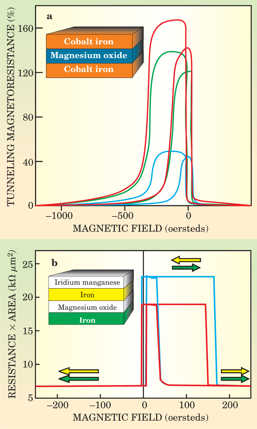
The IBM researchers found the highest TMR with CoFe alloys that were predominantly cobalt, rather than with pure iron. As seen in the top panel of figure 3, TMR increased with the annealing temperature. Also seen in figure 3 is the hysteresis loop associated with the magnetization of the upper layer. The highest values of TMR measured by the IBM group were 220% at room temperature and about 300% at low temperatures. TMR is measured at low bias voltages, around 10 millivolts. Practical devices operate at higher bias voltages, and TMR drops with the bias voltage. Parkin remarked, however, that the decrease was not very great.

Figure 3. Tunneling magnetoresistance as a function of magnetic field. (a) Data from IBM Almaden. The three curves shown are for annealing temperatures of 120°C (blue), 360°C (green) and 380°C (red). Hysteresis loops are seen for all three. (Adapted from ref.
The IBM researchers also found that the electrons tunneling through their device had an 85% spin polarization. This high value may make the tunneling junctions useful as spin injectors in spintronics applications, where the information is carried by the spin rather than the charge.
Parkin says that the MTJs made by his group are thermally stable up to 400°C. While the devices described in their recent paper were quite large—80 microns on a side—Parkin reports that his team has also built submicron-sized junctions with similarly high TMR. The experimenters exploit a phenomenon known as oscillatory exchange coupling to build MTJ structures useful for MRAM applications with a “synthetic artificial antiferromagnetic” reference layer that compensates for the fringing fields from the reference layer that can be a problem as the junction size is greatly reduced. 1
Epitaxial growth
The group from Japan’s AIST grew its MTJs epitaxially, using MBE. This method is certainly not suitable for mass production but the precise control yields crystals that can be used to study the basic physics of the TMR effect. In that sense, Yuasa feels that his team’s results complement those of the IBM group.
Yuasa and his coworkers initially reported
13
a TMR of 88%. More recently they have been able to improve the crystallinity of the upper iron electrode by growing it at temperatures above room temperature. That also helped reduce the excess of oxygen atoms on the top surface of the MgO layer. With those improvements, the TMR rose to 180%. A transmission electron microscope image of the resulting junction is shown in figure
The AIST group also reports evidence of coherence in the spin-polarized tunneling. The theoretical papers had predicted that interference effects stemming from this coherence might cause the measured values of TMR to oscillate as a function of the thickness of the MgO layer. Butler remarked that he and his colleagues never dreamed that anyone would be able to measure that. But the AIST team presents evidence for it.
Yuasa says that he and his fellow researchers are now trying to fabricate a lower-impedance junction for read heads. They are also trying to enhance the TMR effect and to use currents to reverse the direction of magnetization in the MTJs with MgO barriers, for use in write operations.
References
1. For a review, see S. S. P. Parkin et al., Proc. IEEE 91, 661 (2003).https://doi.org/10.1109/JPROC.2003.811807
2. M. Jullière, Phys. Lett. 54A, 225 (1975).
3. For a review, see R. Meservey, P. M. Tedrow, Phys. Rep. 238, 173 (1994).https://doi.org/10.1016/0370-1573(94)90105-8
4. J. S. Moodera, L. R. Kinder, T. M. Wong, R. Meservey, Phys. Rev. Lett. 74, 3272 (1995).https://doi.org/10.1103/PhysRevLett.74.3273
5. T. Miyazaki, N. Tezuka, J. Magn. Mag. Mat. 139, L231 (1995).https://doi.org/10.1016/0304-8853(95)90001-2
6. D. Wang, C. Nordman, J. M. Daughton, A. Qian, J. Fink, IEEE Trans. Magnetics 40, 2269 (2004).https://doi.org/10.1109/TMAG.2004.830219
7. S. S. P. Parkin, C. Kaiser, A. Panchula, P. M. Rice, B. Hughes, M. Samant, S.-H. Yang, Nature Materials, in press (2004).
8. S. Yuasa, T. Nagahama, A. Fukushima, Y. Suzuki, K. Ando, Nature Materials, in press (2004).
9. W. H. Butler, Z.-G. Zhang, R. C. Schulthess, J. M. MacLaren, Phys. Rev. B 63, 054416 (2001).https://doi.org/10.1103/PhysRevB.63.054416
10. J. Mathon, A. Umerski, Phys. Rev. B 63, 220403 (2001).https://doi.org/10.1103/PhysRevB.63.220403
11. Ph. Mavropoulos et al., Phys. Rev. Lett. 85, 1088 (2000).https://doi.org/10.1103/PhysRevLett.85.1088
12. M. Bowen et al., Appl. Phys. Lett. 79, 1655 (2001).https://doi.org/10.1063/1.1404125
13. S. Yuasa et al., Jpn. J. Appl. Phys. 43, L588 (2004).https://doi.org/10.1143/JJAP.43.L588


