Hydrogen Adsorbed on Silicon Carbide Creates Metallic Surface States
DOI: 10.1063/1.1595042
Silicon is the workhorse of the microelectronics industry. But it has its limitations. Researchers who demand high-temperature, high-voltage, and high-frequency properties in their semiconductors turn instead to a sister material, silicon carbide. Thanks to its larger band gap, SiC remains semiconducting at much higher temperatures, melts at 2800°C, and has a hardness exceeded only by diamond.
Now, researchers led by Patrick Soukiassian of the Atomic Energy Commission (CEA) in Saclay, France, and Yves Chabal of Rutgers University have discovered what could turn out to be another advantageous property of SiC: When its surface is exposed to hydrogen atoms, it spontaneously forms two-atom-wide rows of metallic character. 1 That effect was a surprise. “I’ve never heard of adsorption causing surface states—specifically, dangling bonds—to appear,” says Victor Bermudez of the Naval Research Laboratory. “It’s supposed to remove them—it always does.”
Reconstructed surfaces
The newly discovered metallic states exist only on the surface, where electronic properties differ from those of the bulk material. To appreciate the difference, consider what happens when you cleave a crystal along one of its planes. The periodic bulk lattice ends abruptly, which creates intrinsic surface states localized on the topmost layer of atoms. Those electronic states arise from dangling bonds or half-filled orbitals.
In response to the dangling bonds, surface atoms adjust the way they bond to their neighbors in an effort to minimize the total energy. The adjustment can take several forms. Surface atoms can move up or down the surface normal (termed “lattice relaxation”), alter their valence charge density (termed “electronic relaxation”), or move in the surface plane (termed “reconstruction”) to produce new bonding configurations. One consequence of reconstruction is the formation of a quasi-two-dimensional surface unit cell whose size and symmetry can be quite different from those of the unreconstructed unit cell.
The effect of such rearrangement can be profound. For example, silicon’s densest plane, (111), adopts a complicated reconstruction in which the 49 dangling bonds in each (7 × 7) grouping of surface atoms combine to leave just 19 dangling bonds. Reliably predicting such reconstructions a priori is extremely challenging. It took 20 years to resolve the (7 × 7) surface structure of Si(111).
An intricate reconstruction is also behind SiC’s metallic state. Soukiassian, Chabal, and their colleagues have focused on the (3 × 2) structure, one of several known reconstructions of the cubic SiC(100) surface. This structure is based on a three-layered Si-rich arrangement, derived from the adsorption of “excess” Si on the bulk SiC lattice. Figure 1a depicts the reconstruction. Silicon atoms form rows of tilted Si—Si dimer bonds (top layer); those rest on dimers (second layer) that are rotated 90° in the plane and contain two different bond lengths. Both of those layers are arranged on top of a full Si monolayer bonded to carbon.

Figure 1. The reaction of silicon carbide with atomic hydrogen creates a one-dimensional chain of metallic surface states. Atomic models distinguish a clean SiC(100) (3 × 2) surface from a hydrogen-covered one. (a) A top (red/pink) adlayer of tilted Si-Si bonds (dimers) covers a second layer of Si dimers (orange/yellow) oriented orthogonal to the first layer. A third monolayer of Si atoms (silver) bonds to a layer of carbon (black). (b) Atomic hydrogen (white) ties up (“passivates”) the singly occupied dangling bonds on the clean-surface dimers (effectively untilting them) and breaks the third-layer weak dimer bond. That bond-breaking leaves one Si atom available to form a Si—H bond, and leaves the other atom caged in by the geometry. Such blocking stabilizes the newly formed dangling bond on the Si.
(Adapted from ref. 1.)
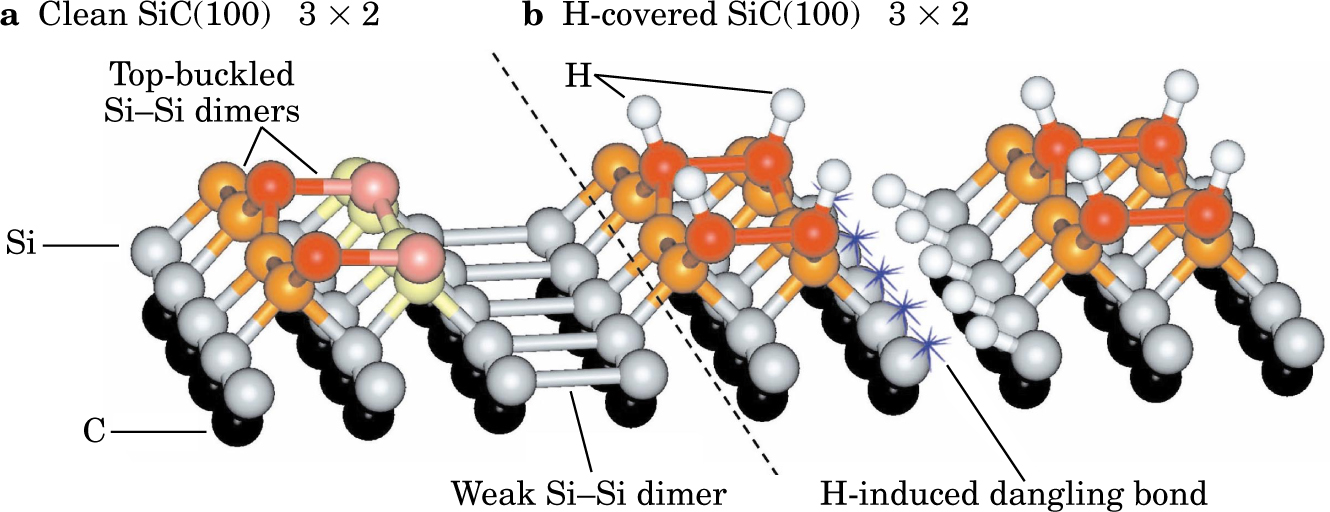
What makes the geometric relation of the layers intriguing—and an essential ingredient in the reaction with hydrogen, it turns out—is the very large (20%) mismatch between the SiC and silicon lattice spacings. The stress effectively compresses the Si dimer layers and influences the electronic structure of the surface.
Simple electron counting shows that the top-layer Si atoms each have one unpaired electron in a dangling orbital. Such partially filled states must cross the Fermi level and would create a metallic surface (that is, one with no gap separating valence and conduction bands) were it not for the dimer’s tilt with respect to the surface plane. Four years ago, Johannes Pollmann of the University of Münster in Germany and colleagues showed that the tilting is accompanied by a bonding-antibonding interaction between the dangling orbitals. 2 This is an example of electronic relaxation, as a result of which a bandgap opens up to give a semiconducting surface with no states at the Fermi level.
Detective work
Originally, Soukiassian and his PhD student Vincent Derycke were trying to understand the Si-rich (3 × 2) surface. As part of that investigation, they exposed the surface to atomic hydrogen, which invariably serves to tie up—that is, “passivate” or “quench”—dangling surface bonds. The use of hydrogen (or a host of other adsorbates) to passivate semiconductor surfaces goes back 30 years. The aim is to create a chemically stable and electrically neutral surface. However, when Derycke used ultraviolet photoelectron spectroscopy (UPS) to monitor changes in electron binding energy of near-bulk and surface atoms, he noticed a remarkable wrinkle: Top-layer dimers were, indeed, terminated with hydrogen, but a fresh new band of surface states also emerged.
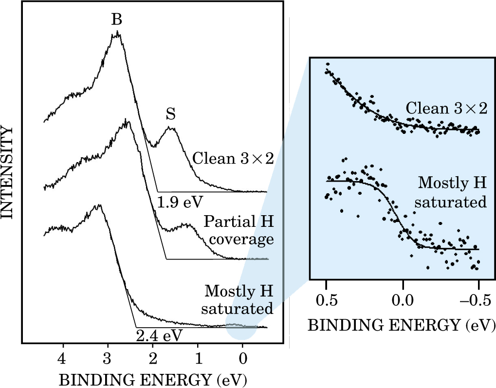
As figure 2 shows, increasing the hydrogen coverage causes the band of surface states, which are evident on clean SiC as the 1.6-eV peak, to move to lower energy and diminish. At saturated coverage, the peak vanishes and a new bump appears at the Fermi level, the highest energy state occupied with electrons.

Figure 2. Photoelectron spectra measure UV-induced emission of electrons located in distinct energy levels (or bands) on the first few surface layers. The gradual disappearance of the 1.6-eV band of surface states (S) with hydrogen exposure is consistent with passivation of the top-layer Si dimers as hydrogen ties up dangling bonds there. The bump at the Fermi level (enlarged in blue) is a signature for a metallic state. The concomitant shift of the valence band maximum (B) toward higher binding energies signals a shift in the surface Fermi level position up to the conduction band edge.
(Adapted from ref. 1.)
In the hope of identifying which atomic structure causes the photoemission peak at the Fermi level, the researchers turned to scanning tunneling microscopy. As an atom-resolving tool, the STM answered only part of the puzzle. Hydrogen exposure untilted the Si dimers in the top adlayer, which made the dimer arrangement symmetric, that is, parallel to the surface. That arrangement is a well-known sign of passivation on Si and it corroborated the disappearing 1.6-eV surface states. However, imaging offered no insight into the bonding rearrangement that could account for the newly emerging peak.
Configuring the STM so that it works as a spectroscopy tool turned out to be a more helpful approach. Scanning tunneling spectroscopy (STS) effectively maps a surface’s electronic structure by measuring the metal-semiconductor tunneling current as a function of voltage. Tunneling from tip to sample occurs only when the tip bias voltage is large enough for the filled states of the metal in the tip to line up with the conduction band of the semiconductor.
As expected for the clean SiC surface, electrons did not tunnel when the tip bias voltage corresponded to an energy between the valence and conduction bands. Once hydrogen began saturating the surface, STS showed the absence of a surface bandgap, consistent with emission at the Fermi level in UPS. Here, then, was a suggestion that the adsorption of H was actually causing the appearance of singly occupied dangling orbitals, where none existed on the bare surface. The precise origin of the state, however, remained a mystery.
To understand that aspect of the puzzle, Soukiassian sought the help of his collaborators, Chabal and Fabrice Amy, then at the Murray Hill, New Jersey research labs of Agere Systems. Chabal and Amy used infrared absorption spectroscopy (IRAS) to diagnose what mechanism could account for atomic bonding changes. Ordinarily, IRAS measures the vibrational stretches that are frequency fingerprints of a particular type of bonding. Amy’s data confirmed that, initially, hydrogen passivates surface dimer rows (H-Si-Si-H), as inferred from STM and UPS. However, using IRAS to measure low-energy electronic transitions, Amy observed a broadband electronic transition extending over the entire accessible frequency range. That low-energy absorption continuum is a signature for the excitation of electrons across the Fermi level of a metal.
Amy and Chabal also observed an unusual vibrational stretch associated with H attached to a Si—C bond in the third layer. That observation turned out to be a critical clue. According to the (3 × 2) model, the formation of any additional Si—H bonds must be contingent on the breaking of the weak Si—Si bonds in the sublayer trough above the carbon plane, shown schematically in figure 1b.
However, if H bonds with one of the Si atoms, the crowded arrangement in that sublayer plane prevents H from reaching the other side of the broken dimer bond. That resulting dangling bond constitutes the metallic state indirectly evident in the STS and UPS spectra.
Designer defects
The blocking effect, known as steric hindrance, is a consequence of the large compressive strain between the bulk layers of SiC and the Si-rich surface layers. The resulting strain appears to be the essential ingredient for stabilizing the dangling bonds that are responsible for the metallic band appearing at the Fermi level. The model in figure 1b renders those dangling bonds (marked by asterisks) as one-dimensional features.
Researchers have metallized surfaces before: Local STM-induced desorption of H—used to create nanopatterns and metallic wires on H-passivated Si—is an example. 3 However, Soukiassian and Chabal’s work demonstrates the controlled creation of spatially localized atomic defects that can, in principle, extend over the entire surface.
But such defects aren’t necessarily equivalent to 1D conducting wires. Indeed, the rows of metallic defects could act more like a polarizing grating than a grid of conducting wires.
To ascertain the metallic character of the defects, Chabal illuminated the surface with polarized infrared radiation. He found that electrons were not excited by the infrared field polarized along the row of defects. That observation contradicts the 1D-wire picture and is more consistent with the model of a complex electronic transition from a dangling bond to the conduction band minimum. Measuring conductivity is an item on the experimental to-do list, but presents enormous challenges. At most, there would be just one electron per atom in half of one full plane available for conduction.
Conductivity aside, the demonstration of a weakly stabilized Fermi level offers hope to those interested in making reliable SiC ohmic contact with other molecules or devices. The presence of a metallic component in an intrinsically insulating substrate like SiC might facilitate charge transport from SiC to an external metal contact.
Soukiassian and Chabal are also trying to determine whether the dangling bonds really fall on just one side of the trough (as rendered in figure 1b) or whether a random pattern is more likely. In any case, at some range of temperatures, they expect hydrogen to hop between the third-layer dimers in a way that would smear out the 1D line of electronic states. That effect—hydrogen hop-ping—could lead to interesting physics itself and provide a basis for studying 1D behavior.
References
1. V. Derycke, P. G. Soukiassian, F. Amy, Y. Chabal, M. D. D’Angelo, H. B. Enriquez, M. Silly, Nat. Mater. 2, 253 (2003) https://doi.org/10.1038/nmat835 .
2. W. Lu, P. Krüger, J. Pollmann, Phys. Rev. B 60, 2495 (1999) https://doi.org/10.1103/PhysRevB.60.2495 .
3. E. T. Foley, A. F. Kam, J. W. Lyding, Ph. Avouris, Phys. Rev. Lett. 80, 1336 (1998) https://doi.org/10.1103/PhysRevLett.80.1336 .


