Graphene production goes industrial
DOI: 10.1063/1.3480063
A single plane of carbon atoms, graphene was isolated in 2004 through a method that could hardly be more low-tech: The University of Manchester’s Andrey Geim and colleagues used common cellophane tape to peel off weakly bound layers from bulk graphite. Once gently rubbed onto an oxidized silicon surface, the rare graphene flakes were then spotted among macroscopically thick graphite pieces in the interference patterns of an optical microscope image. Because it yields nearly defect-free crystals, that time-consuming process has largely remained the method of choice, particularly among researchers exploring the material’s astonishing two-dimensional electron-gas physics (see the article by Geim and Allan MacDonald in Physics Today, August 2007, page 35 ).
Despite the material’s low-tech beginnings, much of its allure lies in the advantages it brings to high-tech applications. Graphene can sustain current densities a million times higher than copper, exhibits record strength and thermal conductivity, is impermeable to gases, is 97% transparent at optical frequencies, and can be elastically stretched by as much as 20%. 1
The challenge of harnessing such rich properties—in a solar cell or a tough but flexible touch screen, say—lies in synthesizing a continuous graphene sheet large enough and conductive enough. Unfortunately, exfoliating a chunk of graphite isn’t a scalable technique—at least for making high-quality (low-resistance) graphene films. One promising approach is to epitaxially grow a graphene layer atop some other crystal. Once the epitaxial layer has cooled, the underlying crystal can then be chemically etched away.
Two years ago, three independent groups—one led by University of Houston’s Qingkai Yu and Purdue University’s Yong Chen, another by MIT’s Jing Kong, and a third by Byung Hee Hong of Sungkyunkwan University (SKKU) in South Korea—did just that, using chemical vapor deposition of methane to catalyze the growth of a few layers (typically less than 10) of graphene on polycrystalline nickel. The graphene was then patterned lithographically or transferred onto square-centimeter wafers of glass, Si, or plastic. 2 The high solubility of carbon in Ni, however, led to wide variations in the graphene’s thickness, a problem the researchers could only ameliorate by rapidly cooling the samples and restricting themselves to thin Ni films.
Shortly thereafter, Rodney Ruoff and colleagues at the University of Texas at Austin solved the problem by replacing Ni with Cu foil, whose carbon solubility is negligible. 3 The replacement allowed them to grow a single layer of graphene over 95% of a 3-cm2 Cu surface.
Hong’s group, in close collaboration with Samsung (which manages SKKU), has now adapted that Cu-based chemical-vapor-deposition growth to a scalable, industrial manufacturing process, as outlined in figure 1. The researchers also chemically doped their graphene film, which increased its conductivity by a factor of four. 4 As proof of principle, they produced a 76-cm-diameter electrode whose conductivity and transparency surpass those of the commercial standard, indium tin oxide, a material that’s expensive and brittle but common in touch screens and computer monitors.

Figure 1. Roll-to-roll production. Chemical vapor deposition of methane on copper foil at 1000°C triggers the catalytic growth of graphene. The graphene-laden Cu is pressed against a flexible polymer support, bathed in an etchant that removes the Cu backing, and then dry transferred to a target—typically another flexible polymer. Multiple layers of graphene, grown one at a time, can be transferred to that target and stacked together—each layer chemically doped in a bath stage similar to that used for etching. The complete process produces a large, flexible, highly conductive, transparent electrode.
(Adapted from
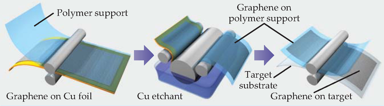
The flexibility of the Cu foil and graphene make both potentially amenable to an automated roll-to-roll production strategy. And when Cu is heated, its grain size increases from microns to millimeters, a step that lowers graphene’s resistivity, Hong argues, by reducing the number of electron-scattering grain boundaries that form in it.
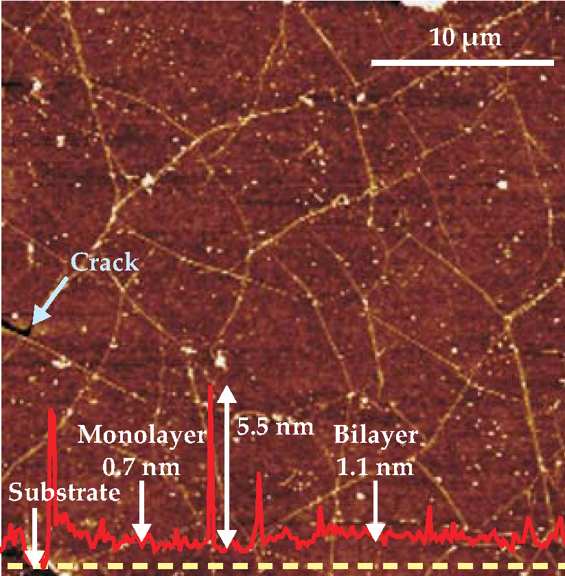
According to Ruoff, during growth at 1000 °C, close to Cu’s melting point, carbon atoms nucleate at various sites across the surface and grow into 2D islands whose honeycomb lattice structures eventually merge, most likely in random orientations. As both materials cool, their mismatch in thermal-expansion coefficient causes the graphene sheet to severely wrinkle, as pictured in figure 2, to relieve the stress caused by Cu’s greater contraction. The sheet can also develop nanoscopic cracks when it’s transferred to a flexible target substrate in the last step of the team’s fabrication process.

Figure 2. Force microscopy reveals the polycrystalline surface of graphene with its network of wrinkles (white lines) and minor cracks that develop during the mild trauma of cooling and being transferred to a substrate. (White dots are most likely polymer residue.) The height profile (solid red line) of graphene and its wrinkles is measured relative to the substrate along the dashed yellow line. Although a single layer of graphene generally predominates when grown on copper, a graphene bilayer is also evident in the scan.
(Adapted from
Unless engineered otherwise—cut into ribbons, for instance, or deliberately strained to alter its band structure—graphene is a zero-bandgap semiconductor. Exposure to a strong Cu etchant such as iron chloride naturally dopes the graphene with holes. But to further increase the charge-carrier density, and thus the conductivity of its films, the SKKU group stacked together four separately grown graphene monolayers, each hole-doped again using nitric acid in the same production process. Unlike in graphite, the hexagonal lattices of adjacent stacked graphene layers are randomly oriented, and the overall conductivity in the graphene film appears to be proportional to the number of stacked layers. Those layers, moreover, may also provide additional conductive channels that bridge the gap between any cracks.
The carrier mobility of the SKKU single-layer films measured about 5000 cm2/V°s at room temperature—close to that of mechanically cleaved graphene. That and the group’s observation of a half-integer quantum Hall effect in graphene, Hong says, are signatures of the films’ high quality. Even so, several research groups are working to resolve ambiguities in the 2D growth process and to understand the influence of graphene’s defects on its electron-transport properties.
Geim remains enthusiastic. “Don’t be surprised,” he says, “if your next mobile phone has a touch screen and an LED light, both containing graphene electrodes.”
References
1. A. K. Geim, Science 324, 1530 (2009); https://doi.org/10.1126/science.1158877
Y. Zhu et al., Adv. Mater. (in press), https://doi.org/10.1002/adma.201001068.2. Q. Yu et al., Appl. Phys. Lett. 93, 113103 (2008); https://doi.org/10.1063/1.2982585
A. Reina et al., Nano Lett. 9, 30 (2009); https://doi.org/10.1021/nl801827v
K. S. Kim et al., Nature 457, 706 (2009). https://doi.org/10.1038/nature077193. X. Li et al., Science 324, 1312 (2009); https://doi.org/10.1126/science.1171245
see also X. Li et al., Nano Lett. 9, 4359 (2009). https://doi.org/10.1021/nl902623y4. S. Bae et al., Nat. Nanotechnol. (in press), https://doi.org/10.1038/nnano.2010.132.


