Two-dimensional van der Waals materials
DOI: 10.1063/PT.3.3297


“What could we do with layered structures with just the right layers?” asked Richard Feynman in his famous 1959 lecture, “There’s plenty of room at the bottom.” With the help of the amazing developments of the past several years, we are coming close to answering that question. Whereas thin layers and multilayers of various kinds have long been known to technology, researchers are now learning to create uniform, atomically thin layers and manipulate them into novel solids with a broad range of physical properties.
Layered materials are characterized by extended crystalline planar structures held together by strong in-plane covalent bonds and weak out-of-plane van der Waals forces. Individual layers can easily be removed by breaking the van der Waals bonds, with little damage either to the remaining structure or to the extracted layer. For example, layers of graphene can be peeled away from bulk graphite with adhesive tape. Hence layered materials can be transferred to any substrate with relative ease.
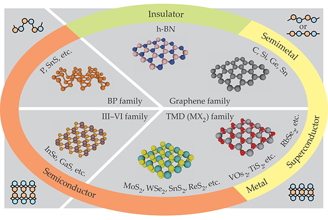
Graphene is one of the most alluring two-dimensional materials because of its unique band structure and exceptionally high carrier mobilities. (See the article by Andre Geim and Allan MacDonald, Physics Today, August 2007, page 35 .) With the discovery that graphene can be controllably grown on metal surfaces by vapor-phase deposition from hydrocarbon precursors, scalable graphene-based technologies started to look more feasible. 1 However, graphene is not the best 2D material for every application—its zero bandgap renders it rather useless as a semiconductor, for example. Fortunately, a large number of other layered materials span the entire spectrum of electronic properties, as shown in figure 1. Among them, hexagonal boron nitride (h-BN) is an insulator with a bandgap exceeding 5 eV, and the family of transition-metal dichalcogenides (TMDs) includes several semiconductors with bandgaps ranging from 0.5 eV to 3 eV. By exploiting the material properties of the layers in isolation or by mixing and matching them to create new structures with atomically thin heterojunctions, researchers are exploring interesting new physics and engineering new ultrathin devices.

Figure 1. The world of two-dimensional materials includes graphene and its analogues, such as hexagonal boron nitride; black phosphorus (BP) and its analogues; the III–VI family of semiconductors; and the transition-metal dichalcogenides (TMDs). Together they span the full range of electronic properties. The four corner diagrams show the materials’ cross-sectional structures—most are not strictly planar.
Physics in two dimensions
Reducing the dimensionality of a system is often associated with exceptional electronic, optical, and magnetic properties, as the reduction of available phase space and diminished screening lead to enhanced quantum effects and increased correlations. Even before the discovery of stable 2D materials, the condensed-matter community extensively investigated the physics of quasi-2D systems, including cuprate high-temperature superconductors, whose superconductivity is confined to planar CuO2 layers, and semiconductor interfaces that host the fractional quantum Hall effect.
The peculiar nature of low-dimensional systems is more apparent in atomically thin materials, and indeed, graphene’s unique electronic properties stem from its reduced dimensionality. The quantum mechanical description of the electronic band structure can be simplified by introducing quasi-relativistic particles near the corners of the Brillouin zone, as shown in figure 2a. At the Brillouin-zone corners, marked K and K′, the valence and conduction bands meet in conical valleys: Energy (represented by the vertical dimension) is directly proportional to momentum (represented by the horizontal dimensions), a relationship reminiscent of massless particles that travel at the speed of light, independent of their energy or momentum. Graphene’s quasiparticles therefore move like electrons that have lost their mass, except that the speed of light is replaced by graphene’s Fermi velocity, which is some three hundred times smaller.

Figure 2. Lattice structures and band structures at the corners of the first Brillouin zone for (a) monolayer graphene, (b) bilayer graphene, (c) hexagonal boron nitride, and (d) the transition-metal dichalcogenides (TMDs). The dashed lines in the lattice diagrams indicate unit cells. Because of their inversion symmetry, monolayer and bilayer graphene have no bandgap. Due to spin–orbit coupling, the TMDs’ valence band is split into two spin-polarized bands, marked by the red and blue arrows.
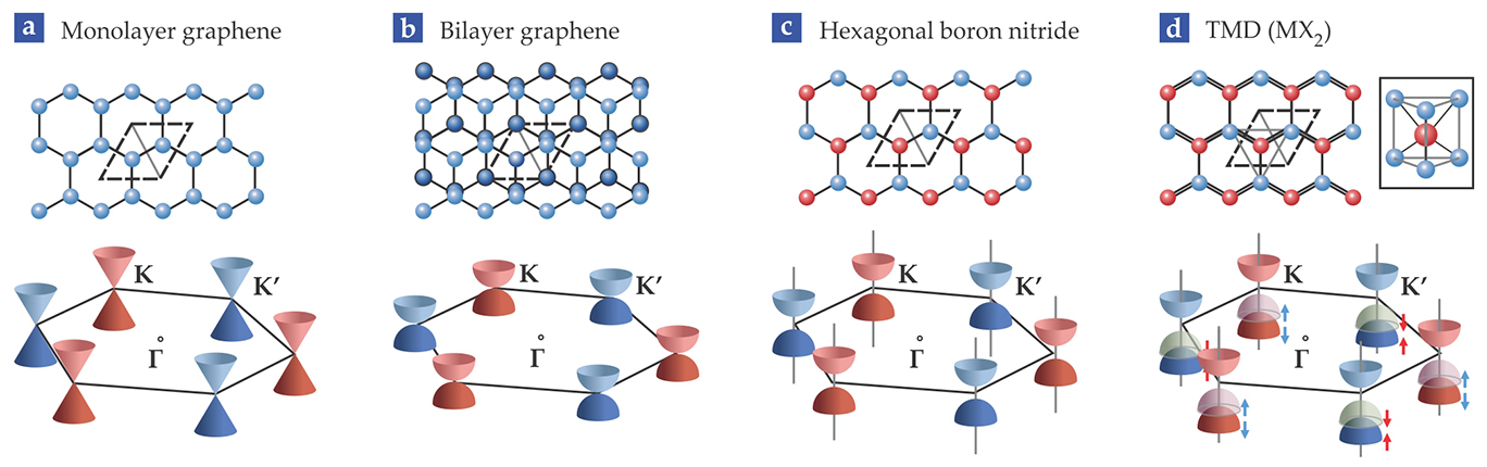
In real relativistic spin-½ fermions, such as neutrinos, the spin must be either parallel (right handed) or antiparallel (left handed) to the particle’s momentum. Graphene’s quasiparticles have an analogous pseudo-spin degree of freedom, which describes the wavefunction symmetry on the two triangular sublattices of graphene’s hexagonal lattice: Depending on whether the quasiparticle sits in a K or a K′ valley, the pseudo spin is either parallel or antiparallel to the momentum. From that chiral nature of charge carriers, various electronic properties emerge, such as a half-integer shift in the quantum Hall effect and so-called Klein tunneling across an arbitrarily large potential barrier. Graphene was also the first system in which a nontrivial Berry phase could be detected experimentally, a discovery that supplied an important connection to the later discovery of topological insulators. 2
In bilayer graphene, shown in figure 2b, two graphene layers stack together to form a staggered honeycomb lattice. Its quasiparticles gain a mass, and the energy dispersion becomes parabolic. The inversion symmetry of bilayer graphene keeps the energy degeneracy at the K and K′ valleys and prevents a bandgap from opening. That degeneracy can be lifted by breaking the lattice’s inversion symmetry. For example, in h-BN, shown in figure 2c, the two carbon atoms in the graphene unit cell are replaced by boron and nitrogen, and the inversion symmetry is broken. As a result, a large energy gap opens at the valleys, making h-BN an extremely good insulator and dielectric.
The TMDs are a particularly interesting class of 2D materials. Their crystal structure, shown in figure 2d, consists of one layer of a transition metal M, such as molybdenum or tungsten, sandwiched between two layers of a chalcogen X, such as sulfur, selenium, or tellurium. A single 2D unit consisting of those three atomic layers is about 6–8 Å thick. The TMDs have no inversion symmetry, and most of them have nonzero bandgaps. But their band structure is complicated by strong spin–orbit coupling, which arises from the high orbital velocities in the relatively heavy M atoms’ partially filled d subshells. That spin–orbit coupling splits the TMDs’ valence bands into two spin-polarized bands. Time-reversal symmetry requires the spin and momentum degrees of freedom to be coupled such that the K and K′ valleys carry opposite spin polarizations. That unique spin and valley texture causes electrons to experience a pseudo-magnetic field, which gives rise to a so-called valley Hall effect even in the absence of an applied field. Furthermore, by applying circularly polarized light, researchers can control both the electrons’ spin and the momentum valley they occupy. 3
Quantum confinement and the lack of bulk dielectric screening have profound effects on the optical properties of semiconducting TMDs. For example, many bulk TMDs have indirect bandgaps: The valence-band maximum and conduction-band minimum are characterized by different wavevectors. But in monolayer form, the materials undergo a transition to a direct bandgap, which results in stronger optical absorption and more efficient radiative recombination. Figure 3a shows the effect for MoS2. Additionally, excitons—electron–hole pairs created by single-photon absorption—can have large binding energies in 2D TMDs due to the lack of bulk dielectric screening.

Figure 3. The unique physics of two-dimensional materials. (a) The band structure is shown of molybdenum disulfide in bulk (black and gray) and monolayer (red) forms. The valence-band maximum Ev and conduction-band minimum Ec correspond to different wavevectors in bulk but the same wavevector in the monolayer. (b) In the anisotropic band structure of black phosphorus, the effective carrier masses m* in the x and y directions both differ from the electron mass m0. (c) A quasiperiodic moiré pattern is formed when graphene (black) and hexagonal boron nitride (red) are stacked at an arbitrary angle θ. (d) The fractal energy spectrum of the structure in panel c is an experimental realization of Hofstadter’s butterfly. (e) Shown here are the schematic structure and band diagram of a photoexcited, atomically thin p–n junction. (Panels c and d adapted from ref.
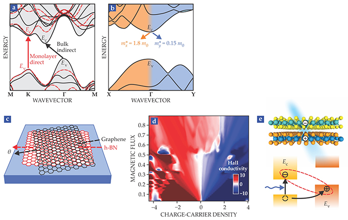
Black phosphorus (BP), or phosphorene, a layered allotrope of elemental phosphorus, has some interesting properties that arise from its inherent in-plane anisotropy. As shown in figure 1, BP layers take the form of puckered sheets. Consequently, the material has an anisotropic band structure, and its charge carriers have anisotropic effective mass. As figure 3b shows, the effective charge-carrier mass in the x direction, perpendicular to the puckers, is 12 times the effective mass in the y direction, parallel to the puckers. The anisotropy couples to lattice strain and is being investigated for applications such as low-dimensional piezoelectricity. Some other layered semiconducting materials, such as rhenium disulfide, exhibit similar anisotropy.
Stacking layers
The recent rise of van der Waals material systems raises the possibility of new types of quantum heterostructures with atomically sharp interfaces between 2D layers of dissimilar materials. 4 Stacking two or more atomic layers of different van der Waals materials compounds the rich variety of 2D electronic systems and allows researchers to explore novel collective quantum phenomena at the interfaces. Electrons’ correlation with spins, phonons, and other electrons can be greatly increased, which affects the transport of charge, entropy, and energy in the quantum limit. Due to the limited phase-space volume, quantum fluctuations are often enhanced and compete with long-range order. As a result, van der Waals heterostructures may exhibit emergent phenomena: Interlayer excitons—electrons in one layer bound to holes in another—may condense into a superfluid, and the coupling between layers may give rise to exotic triplet superconducting states.
The twisting angle between two 2D materials, as shown in figure 3c, is an additional degree of freedom in assembling van der Waals heterostructures: Adjusting the angle between two atomic lattices can result in structures with different properties. Strictly speaking, two lattices stacked with an arbitrary twisting angle between them do not form a periodic lattice, except at particular discrete angles when the two lattices form a periodic, or commensurate, structure. However, even incommensurate heterostructures can form large-scale quasi-periodic moiré patterns, such as the one shown in figure 3c. The physical properties of heterostructures often sensitively depend on interfacial commensurability, so tuning the twisting angle allows researchers to engineer a large number of combinations of van der Waals materials.
One example of the new interfacial phenomena being explored is the experimental realization of Hofstadter’s butterfly. 5 As Douglas Hofstadter predicted in 1976, a butterfly-shaped fractal energy spectrum emerges when electrons confined to a 2D sheet are subjected to both a periodic energy potential and a strong magnetic field. Past experimental attempts to study the butterfly used artificial structures to create the required periodic potential. But in 2013 three groups, including one led by one of us (Kim), achieved quasi-periodic potentials with the moiré pattern between a layer of graphene and a substrate of h-BN. Although h-BN and graphene are atomically dissimilar, their lattice constants differ by only a few percent, so they form an atomic-scale moiré pattern with a periodic potential. The energy spectrum was then mapped by measuring the electrical conductivity of the heterostructure as a function of applied voltage and magnetic field. That measurement revealed the predicted fractal quantum Hall effect, as shown in figure 3d.
A broad variety of other physical effects of both basic and applied interest have been demonstrated or proposed in layered van der Waals materials. Some examples include atomically thin p–n junctions for solar cells (as shown in figure 3e), exciton superfluidity at high temperatures, 6 novel chiral resonant tunneling between misaligned graphene sheets separated by a h-BN barrier, 7 and superconductor–semiconductor interfaces with unusual Andreev reflections and Josephson coupling.
Materials synthesis
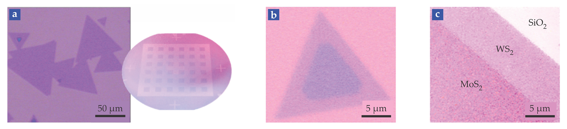
To fully exploit the potential of van der Waals heterostructures, materials scientists must rise to the task of growing atomically thin materials uniformly. Because of significant recent progress, graphene monolayers can be grown on both metallic and nonmetallic substrates, from various hydrocarbon precursors, and even roll to roll. 8 (See Physics Today, August 2010, page 15 .) Several other 2D materials can also be synthesized by chemical vapor deposition with good control and uniformity; figure 4a shows some results for MoS2. In general, TMDs can be grown at the wafer scale by vapor-phase epitaxy methods such as molecular-beam epitaxy and metalorganic chemical vapor deposition. 9 Figures 4b and 4c show atomically precise heterojunctions, both vertically stacked and in plane, made from MoS2 and WS2 by chemical vapor deposition. 10 Advances in 2D materials synthesis have been supported by significant developments in characterization methods, such as Raman spectroscopy and photoluminescence techniques, to determine the number of layers in a sample and how they stack together.

Figure 4. Transition-metal dichalcogenides (TMDs) synthesized by chemical vapor deposition. (a) Shown here are crystal grains (left) and wafer-scale synthesis (right) of molybdenum disulfide. (b) In this vertical heterojunction of two TMDs, the large triangle is a crystal of MoS2, and the small triangle is a crystal of tungsten disulfide grown on top. (c) In an in-plane heterojunction, crystals of MoS2 and WS2 are grown side by side on a silicon dioxide substrate. (Panels b and c adapted from ref.
It remains a challenge to grow 2D structures that are intrinsically unstable or stable only in specific isomeric structures. Particularly difficult are layered materials with nonlayered counterparts, such as phosphorene, silicene, stanene, germanene, and borane. However, for layered materials that are stable in bulk, including graphene, h-BN, and the TMDs, it is possible to bypass vapor-phase synthesis by exfoliating the bulk materials to obtain monolayer and few-layer dispersions in solvents. 11 Exfoliation can be done in large quantities, and although it does not produce monodisperse materials, it could be useful for applications such as catalysis and energy storage.
Because almost every atom in a monolayer is exposed to the environment, the material can be extremely responsive to external stimuli and interactions. As a result, many 2D materials are unstable in air and easily oxidize or degrade on exposure to light and moisture. Furthermore, substrate interactions, charge-transfer phenomena, wrinkling, and mechanical instability may induce undesirable changes to a layer’s electronic properties. But chemically modifying the materials in a controlled way can produce beneficial structural changes. As with semiconductors, 2D layers can be doped to modify their bandgaps and electronic structures. Alloying, which can be thought of as an extreme case of doping, may also be possible, although phase diagrams of 2D alloyed materials have not yet been established. Intercalation, the reversible insertion of molecules or ions into a stacked structure, can also change the material’s electronic structure significantly.
Device applications
Because 2D materials span the full range of electronic properties, as shown in figure 1, they can be combined to build various planar electronic devices with high performance, low power consumption, and other desirable properties such as flexibility and transparency. 12 Figure 5 depicts some of the possibilities. Multilayered graphene is a conductor, so it can replace bulk metals, such as aluminum and copper, in an integrated circuit. In a bulk-metal wire carrying an AC signal, the current density is largest near the wire’s surface. That so-called skin effect leads to power loss and heat dissipation. Theoretical analysis has shown that the effect is diminished in multilayer graphene ribbons, which could be promising for designing low-loss devices that can operate at ultrahigh frequencies and low power. For example, one of us (Banerjee) and colleagues recently demonstrated that graphene can be patterned into a spiral inductor.

Figure 5. Electronic and optoelectronic applications of two-dimensional materials. Various 2D components, shown on the left, could one day be integrated into ultrathin layers, as shown on the right.
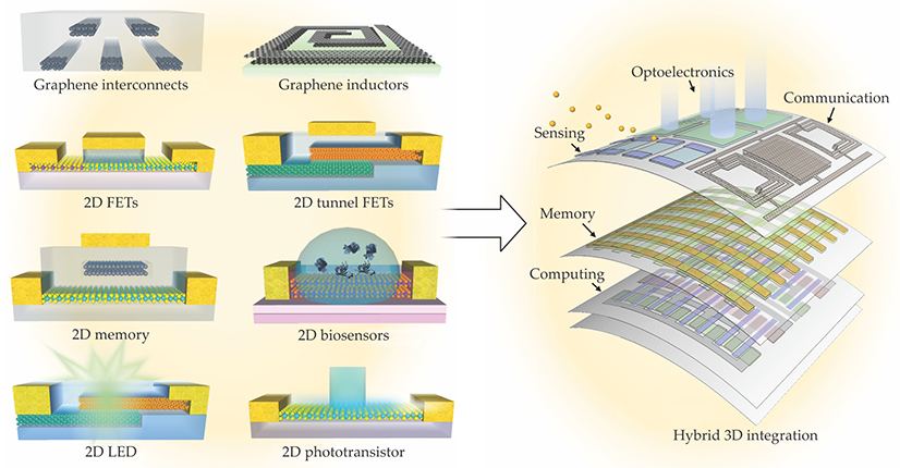
The semiconducting TMDs such as MoS2 and WSe2 have many desirable properties for low-power devices; those properties include uniform thickness, atomically smooth surfaces without dangling bonds, and relatively large bandgaps of 1–2 eV. Because the energy dispersions near the band edges are parabolic in shape, as shown in figure 3a, carrier transport in monolayer TMDs can be described by effective-mass transport equations. Monolayer TMDs generally have larger effective carrier masses than common bulk semiconductors do, so their density of states, which is proportional to the effective mass, is also large. As a result, monolayer TMDs have large mobile carrier densities and thus can carry high currents.
The field-effect transistor is one of the most common electronic components. In any FET, the flow of charge carriers through a semiconducting channel between the source and drain terminals is controlled by a third terminal, the gate. The atomic-scale thickness of 2D semiconductors leads to excellent electrostatic control, which means, importantly, that the gate lengths of 2D FETs can be made smaller. In fact, a rigorous scaling analysis of 2D FETs shows that they have excellent promise for very large scale integrated circuits with sub-10-nm gates. 13
The highly anisotropic 2D layered materials, such as BP and ReS2, provide another attractive platform for FETs with gates smaller than 10 nm. When the material’s low-effective-mass direction is aligned with the FET’s transport direction, the carrier velocity can be significantly enhanced without compromising the density of states or carrier density, and the drive current is thereby improved.
The 2D semiconductors show particular promise for designing tunnel FETs, a new type of transistor known for its potential in ultralow-power applications. TFETs are similar in design to MOSFETs, except that their switching behavior is governed not by thermionic emission but by quantum mechanical band-to-band tunneling through a barrier. As a result, their subthreshold swing, dVgs/dlogIds, where Vgs is the gate-to-source voltage and Ids is the drain current, can be lowered below the theoretical limit of 60 mV per decade for MOSFETs. Essentially, subthreshold swing is inversely related to how quickly a transistor turns on at low voltage: The lower the subthreshold swing, the steeper the turn-on behavior, and the better the device performance. Ultrathin 2D materials help to reduce the tunnel barrier width, thereby increasing the tunneling probability and the turn-on current. Because their surfaces are free from dangling bonds, they can effectively suppress tunneling leakage and further improve the subthreshold swing.
The first 2D-material TFET, called the ATLAS-TFET, combines a bulk germanium source and a 2D MoS2 channel to form a vertical heterostructure. 14 Electrons can be efficiently injected into the 2D channel via tunneling through the extremely thin interface, or van der Waals gap, between the two semiconductors. The device exhibits a subthermionic subthreshold swing over four decades of current at an ultralow power-supply voltage of 0.1 V. If integrated into circuits, it could yield an enormous reduction in power consumption.
Ultralow-power circuitry is central to the emerging paradigm of the Internet of Things, the network of physical devices endowed with sensors, actuators, and other electronics. (See Physics Today, September 2014, page 20 .) Conventional FETs with 2D MoS2 channels have already been proven to make excellent biosensors. 15 The MoS2 surface is functionalized with receptors that bind specifically to the biomolecules of interest, induce a gating effect, and modulate the device current. All the properties of MoS2 that make the MoS2 FET a good transistor—its atomic-scale thinness, pristine surfaces, and considerable bandgap—are instrumental in its performance as a biosensor as well. That parallelism raises the possibility that 2D-channel TFETs, which combine the advantages of an atomically thin 2D channel with the high sensitivity of a TFET, can also be adapted into a revolutionary new class of biosensors.
Some key challenges facing 2D device design are contacts, interfaces to dielectrics, and doping. Due to their layered nature that gives rise to van der Waals bonds to other 2D and 3D materials, 2D semiconductors don’t readily form high-quality electrical contacts. But recent theoretical and experimental advances on the nature of charge transfer across a 2D material interface have helped to establish pathways to the realization of low-resistance contacts. 16 (See also the article by Xinming Li and Hongwei Zhu on page 46 of this issue.) Specifically, the contact resistance across a van der Waals–bonded interface depends both on the tunneling of charge carriers across the van der Waals gap and on the Schottky barrier that exists at any metal–semiconductor junction. On the other hand, so-called seamless electrical contacts, such as the covalently bonded in-plane interfaces between different 2D materials, provide a promising way to lower contact resistances.
Feynman’s dream come true
Atomically thin materials have the potential to revolutionize technologies from nanoelectronics to optoelectronics and from catalysis to coatings. The ability to control the electronic states of 2D materials is expected to lead to new physical phenomena and device concepts. Furthermore, stable atomic monolayers with various compositions and electronic structures can be stacked in combinatorial ways to produce a large number of layered material systems with as yet unexplored properties. Semiconducting 2D monolayers with direct bandgaps are ideally suited for generating and detecting photons at wavelengths that vary as a function of the bandgaps, which can be tuned through composition, chemistry, or quantum confinement. The confinement could be achieved simply by changing the number of layers, provided that the materials can be synthesized and characterized with atomic precision.
Looking ahead, integration of various 2D circuit elements into 2D logic and memory circuits could be an attractive way to create ultradense, low-power, flexible electronics. It may even be possible to form entire logic circuits from a monolithic sheet of a single starting material—such as graphene, which can be turned from a conductor into a semiconductor either by doping or by patterning it into armchair nanoribbons—and thereby alleviate the need for external contacts. 17 Furthermore, 2D logic and memory layers could be vertically integrated with 2D optics, sensors, and components for energy scavenging and storage, as schematically depicted in the right panel of figure 5, to form compact, energy-efficient devices of ultimate thinness. We are coming ever closer to realizing Feynman’s dream of layered materials—and devices—with just the right layers.

We thank Jiahao Kang of the Nanoelectronics Research Lab at the University of California, Santa Barbara for his assistance in drawing some of the figures.
References
1. X. Li et al., Science 324, 1312 (2009). https://doi.org/10.1126/science.1171245
2. C. L. Kane, E. J. Mele, Phys. Rev. Lett. 95, 226801 (2005). https://doi.org/10.1103/PhysRevLett.95.226801
3. D. Xiao et al., Phys. Rev. Lett. 108, 196802 (2012). https://doi.org/10.1103/PhysRevLett.108.196802
4. A. K. Geim, I. Grigorieva, Nature 499, 419 (2013). https://doi.org/10.1038/nature12385
5. C. R. Dean et al., Nature 497, 598 (2013); https://doi.org/10.1038/nature12186
L. A. Ponomarenko et al., Nature 497, 594 (2013); https://doi.org/10.1038/nature12187
B. Hunt et al., Science 340, 1427 (2013). https://doi.org/10.1126/science.12372406. M. M. Fogler, L. V. Butov, K. S. Novoselov, Nat. Commun. 5, 4555 (2014).
7. M. T. Greenaway et al., Nat. Phys. 11, 1057 (2015). https://doi.org/10.1038/nphys3507
8. S. Bae et al., Nat. Nanotechnol. 5, 574 (2010). https://doi.org/10.1038/nnano.2010.132
9. K. Kang et al., Nature 520, 656 (2015). https://doi.org/10.1038/nature14417
10. Y. Gong et al., Nat. Mater. 13, 1135 (2014). https://doi.org/10.1038/nmat4091
11. V. Nicolosi et al., Science 340, 1420 (2013). https://doi.org/10.1126/science.1226419
12. D. Akinwande, N. Petrone, J. Hone, Nat. Commun. 5, 5678 (2014); https://doi.org/10.1038/ncomms6678
G. Fiori et al., Nat. Nanotechnol. 9, 768 (2014). https://doi.org/10.1038/nnano.2014.20713. W. Cao et al., IEEE Trans. Electron. Devices 62, 3459 (2015). https://doi.org/10.1109/TED.2015.2443039
14. D. Sarkar et al., Nature 526, 91 (2015). https://doi.org/10.1038/nature15387
15. D. Sarkar et al., ACS Nano 8, 3992 (2014). https://doi.org/10.1021/nn5009148
16. A. Allain et al., Nat. Mater. 14, 1195 (2015); https://doi.org/10.1038/nmat4452
J. Kang et al., Phys. Rev. X 4, 031005 (2014). https://doi.org/10.1103/PhysRevX.4.03100517. J. Kang et al., Appl. Phys. Lett. 103, 083113 (2013). https://doi.org/10.1063/1.4818462
More about the authors
Pulickel Ajayan is a professor of materials science and nanoengineering at Rice University in Houston, Texas. Philip Kim is a professor of physics at Harvard University in Cambridge, Massachusetts. Kaustav Banerjee is a professor of electrical and computer engineering at the University of California, Santa Barbara.


