Top-down nanomanufacturing
DOI: 10.1063/PT.3.2621


Nanotechnology is the scientific perfect storm. Over the past several decades, research at the nanoscale in physics, chemistry, and biology has converged to produce some extraordinary breakthroughs. In physics, the feature sizes of semiconductor devices have shrunk, in accordance with Moore’s law, 1 to 22 nm for current commercial products and 5–10 nm for research devices. 2 In chemistry, scientists have moved from thinking about atoms and simple molecules to studying large complexes such as proteins with hundreds of thousands of atoms. In biology, DNA, RNA, and cellular membranes exhibit a remarkable set of capabilities dominated by behavior at the nanoscale.
Nanotechnology comprises devices and structures whose small characteristic dimensions, between 1 nm and 100 nm, result in important functional differences from similar devices at larger scales. Developments of the past 20 years or so include the discovery and synthesis of new materials, such as carbon nanotubes and graphene, and new tools—including atomic force microscopes (AFMs), cold-atom physics, systems-biology techniques, and molecular-beam epitaxy—for studying and manipulating the nanoscopic world.
The next step facing nanotechnologists is determining how to move from laboratory discoveries to commercial products, that is, how to manufacture devices with nanoscale features in a practical, scalable way, at low cost, and with good control over the critical dimensions. Economic realities constrain the space of possibilities as significantly as the laws of nature: At the end of the day, the manufacturing process can’t cost more than the value of the device or system being built. Although an AFM costing a million dollars can certainly be used to build nanoscale transistors one atom at a time, the finished products couldn’t compete with larger-scale transistors, which currently cost nanodollars each.
The challenges of nanomanufacturing are no less daunting than those of nanotechnology research. In this article we discuss some of the approaches being explored and the progress made so far. The work we describe represents a massive undertaking in applied physics, with contributions from disciplines such as materials science, beam physics, quantum optics, micro- and nanomechanics, metrology, statistical analysis, and real-time control systems—just to name a few.
From above and below
Nanomanufacturing techniques can be divided into two groups: top down and bottom up. Bottom-up manufacturing is how chickens are manufactured. Over billions of years, nature has evolved a set of processes whereby information encoded in DNA is used to control, via chemical and biological processes that researchers are only beginning to understand, the construction of complex biological systems with extraordinary functionality. Long-range order is created by local chemical reactions, or local intelligence. The human brain is the quintessential example of what bottom-up engineering can do. Resourceful scientists are now beginning to replace billions of years of trial and error with deductive reasoning to re-create nature’s manufacturing processes.
Our focus in this article is on the top-down approach, in which a global intelligence, or central control, determines what material is placed where. Most nanotechnologists believe that top-down engineering is likely to be the only way to produce microprocessors and memory chips for the next 10–20 years. 3
Nanomanufacturing requires that we think about the problem along two separate axes: device size and throughput. It does little good to produce nanoscale transistors if it would take the age of the universe to make 1010 of them on a single chip. Likewise, throughput is not important if the devices aren’t nanoscale. A viable process must have both high resolution and high throughput.
However, as shown in figure 1, smaller features are almost always slower to manufacture. The relationship of resolution to throughput is described by Tennant’s law, 4 which states that the areal throughput T of a nanomanufacturing process scales with the fifth power of the feature length scale L. As the resolution increases, the number of pixels per unit area scales as L−2. Furthermore, the time required to manufacture a voxel, or three-dimensional pixel, scales as L−3: Small voxels are more time consuming to write than larger ones. Those two relationships combine to yield Tennant’s T = αL5 scaling law. The challenge of nanomanufacturing is to increase the scaling constant α, or possibly find exceptions to the rule.

Figure 1. Nanomanufacturing techniques must not only produce structures on a small length scale L but also achieve a high areal throughput T. Tennant’s law, which states that T scales as the fifth power of L, holds approximately over a wide range of technologies discussed in the text, including those based on scanning tunneling microscopes (STMs) and atomic force microscopes (AFMs), optical lithography, electron-beam (e-beam) lithography and reflective e-beam lithography (REBL), nanoimprinting, focused ion beams (FIBs), dip-pen nanolithography (DPN), and atomic calligraphy. Beating that trend (shifting the black curve down and to the right) is the challenge of nanomanufacturing. (Adapted from refs.
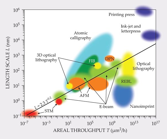
At one end of the curve shown in figure 1 are high-throughput technologies such as ink-jet printing and the letterpress. (The Gutenberg printing press was the disruptive technology that got the ball rolling.) At the other end are lithographic techniques based on AFMs and scanning tunneling microscopes (STMs). With a cantilever and a sharp tip, structures can be built from individual atoms. As we discuss, AFMs can be used in multiple configurations for both imaging and nanomanufacturing, but throughput has always been an issue. 5
Research in top-down nanomanufacturing follows three main themes, which overlap considerably. The first is resist-based nanolithography, the nanoscale extension of techniques similar to the current process of patterning photoresist. The second is nanoimprinting and nanostamping: Think of a nanoscopic rubber stamp, a tool well suited for making many identical copies. The third encompasses direct writing techniques, in which one controls with nanoscale precision when and where atoms are placed.
Resist-based nanolithography
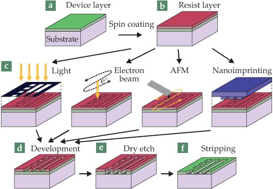
Photolithography has long been the technique of choice for manufacturing semiconductor devices. The basic process is sketched in figure 2. Light passing through a photomask transfers the pattern of the mask to a thin, polymeric photoresist layer, which then transfers it to the device layer underneath. Manufacturers can achieve high throughput by flooding the mask with light, thereby patterning a large area in a short time.

Figure 2. Resist-based lithography. The device layer (a) is spin coated with a thin layer of polymer resist (b). The resist can be patterned using any of a wide range of technologies (c), including photons and a mask, an electron beam, an atomic force microscope (AFM), and a nanoimprint template. The development step (d) removes the exposed area. An anisotropic dry etch (e) removes the unwanted material from the device layer. A final step strips the resist (f) to leave behind the micro- and nanodevices. Multiple iterations of depositions and lithography sequences result in complex multilayered structures.
For finer features one needs shorter-wavelength light. The multidecade trend toward smaller devices has seen photolithography evolve from using visible and UV light, with wavelengths in the hundreds of nanometers, to using extreme UV radiation—really just soft x rays—with a wavelength of 13.5 nm. 6 But shorter-wavelength radiation is both harder to generate and harder to focus. The effective wavelength can be reduced by using two- photon processes: patterning the resist using either a focused light beam or the convergence of two beams. 7 The two-photon approach also allows three-dimensional structures to be written into the photoresist. However, because each feature must be traced out in a serial process, the throughput is much lower than for standard photolithography. Other exotic methods, such as plasmonic nanolithography, can also beat the resolution limit but likewise have a steep penalty in throughput.
To further reduce the wavelength, one must move away from photons and instead pattern the resist using waves of matter, as with electron-beam (e-beam) lithography. The de Broglie wavelength of 100-keV electrons is about 0.001 nm, orders of magnitude smaller than the wavelength of the photons typically used in lithography. The charged electrons can be easily manipulated, and the resolution is no longer limited by the wave nature of the electrons but rather by one’s ability to focus them to a point. Although capable of extreme precision, e-beam lithography raises a host of challenges in terms of throughput. As in a scanning electron microscope, the electron beam is raster scanned over the substrate, so pixels must be written sequentially. Many research labs use e-beam systems to create nanostructures—but in such an environment, throughput is not important.
Commercially, e-beam systems are used to create the photomasks used in optical lithography. The masks take a long time to make, but they can be used hundreds or thousands of times. However, when e-beam systems are used to fabricate the devices themselves, the problem of throughput becomes critical. More sensitive resists allow for faster writing times, but they tend to be lower resolution. Research avenues for extending e-beam lithography for nanomanufacturing include multiple e-beam systems, flood illumination, and faster inorganic resists. 8
Reflective e-beam lithography (REBL) has the potential to overcome the drawbacks of standard e-beam lithography. 9 A huge advantage of the approach is that it does not need or use a physical mask. The desired structure is programmed into a digital pattern generator made up of some 106 independently controllable pixels. A broad electron beam is spatially modulated by the pattern generator to create in the reflected beam a multitude of beamlets operating in parallel. Such massively parallel e-beam systems are serious contenders for next-generation lithography at the nanoscale.
For the finest level of control, one can use an AFM or STM to write a pattern directly into a resist. 10 Heated AFM tips can pattern resists on a gray scale; the range of degrees of exposure is transferred into a range of etch depths in the device layer. Applications include nanofluidics, in which channel dimensions vary in both width and depth. In processes without a traditional resist, the AFM tip can be used to create an etch mask by locally oxidizing the device-layer surface. In a humid environment, the high electric fields that can be generated between an AFM tip and a conducting substrate can cause anodic oxidation. By controlling the oxide thickness, a gray-scale mask can be created; that approach has been used to create microlenses, both concave and convex. In a conceptually similar process, the energetic electrons from an STM tip can locally desorb hydrogen from an H-passivated silicon surface to create regions of oxidation with nanometer precision. Although AFM and STM technologies are intellectually interesting and show what is possible, it is hard to imagine them becoming general-purpose nanomanufacturing processes.
Nanoimprinting and nanoscratching
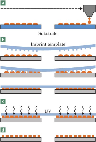
Nanoimprinting, a 21st century implementation of Johannes Gutenberg’s printing press, has much to recommend it. Because large areas can be simultaneously written, its throughput can be 12 orders of magnitude higher than for direct-write approaches. In the example illustrated in figure 3, resist is dispensed using an ink-jet. (It can also be deposited by spin coating.) A template, or mold, then shapes the resist mechanically to create the desired pattern, which is then transferred to the device layer by etching. The resolution is limited by the resolution of the mold, not the photons exposing the resist. Because the mold is used many times, it can be made by a slow but high-resolution method. After that, the speed-limiting factor is the brief time it takes to apply the photoresist.

Figure 3. Nanoimprint lithography, the nanoscale version of a rubber stamp. After the liquid resist (orange) is dispensed onto the substrate (a), the imprint template (b) mechanically molds it into the desired patterns. The resist is cured with UV light (c) to produce the nanoscale pattern (d). (Adapted from ref.
Although the basic idea is simple, nanoimprinting works amazingly well for creating nanoscale features. However, its drawback is that two or more nanoimprinted layers cannot be aligned with nanometer precision. That limitation precludes its use in some applications, including the manufacture of integrated circuits. But in other applications, such as magnetic memory, alignment of layers matters less. Over the next several decades, nanoimprinting may become the dominant technology for creating magnetic memories.
Another technique based on mechanical interactions is AFM-enabled nanoscratching, in which an AFM tip is used to pattern material predeposited on a substrate. In the so-called scratching mode, the cantilever is plowed over the surface but remains essentially static. Alternatively, in an approach known as dynamic plowing lithography, the cantilever can be driven to oscillate up and down at its resonance frequency to chip away at the surface. Because of its low throughput, nanoscratching is not likely to become a general-purpose patterning process, but it could become a valuable manufacturing tool for creating large arrays of magnetic nanodots for high-density storage. The main difference between nanoscratching and other AFM methods is that no chemical reactions take place. Nanoscratching is solely based on mechanical abrasion.
Direct additive techniques
So far we have discussed techniques in which one places much more material on the substrate than is needed and then removes the excess. As devices shrink to comprise a small number of atoms, or even single atoms, that approach fundamentally breaks down: It would be highly impractical, if not technologically impossible, to place many atoms on a substrate and then remove all but a few or one. To solve the problem, researchers have developed direct additive techniques, in which one places the atoms one wants where they are wanted and nowhere else.
One such technique is chemical vapor deposition using focused ion beams. FIB systems are similar to e-beam systems but use ions instead of electrons. The most common ion source is gallium: Its low melting temperature, low vapor pressure, and stable emission characteristics make it ideal. As a rule, lower-mass ions can provide higher resolution, and higher-mass ions offer greater momentum. Because ions are much heavier than electrons, FIBs can be used to etch away, or mill, previously deposited materials. Etch-assist gases activated by the high-energy ions can locally alter the reactivity of specific substrate materials. For example, the presence of water enhances etching of carbonaceous materials such as diamond but decreases the milling rate of silicon.
Likewise, when FIBs are used for chemical vapor deposition, the ions react with a local cloud of an organometallic precursor gas. When exposed to the ion beam, the metal atoms precipitate out of the gas and onto the substrate. The remaining volatile organics are then pumped out of the chamber. Nanostructures can thus be made of materials 11 such as gold (using C7H7O2F6Au as a precursor), platinum (using C9H16Pt), carbon (using C10H8), and tungsten (using W(CO)6). Although highly capable as research tools, FIBs are plagued by the same issues that hamper e-beam systems: high costs and low throughput. The need for liquid-metal ion sources adds another level of complexity and probably makes FIB technology a nonstarter as a production tool. However, FIB-enhanced deposition of platinum is often used in commercial manufacturing to repair errors or correct defects in the masks used for optical lithography. The slow throughput is not a concern when repairing masks that will be used many times, but it is disqualifying for the large-scale production of the devices themselves.
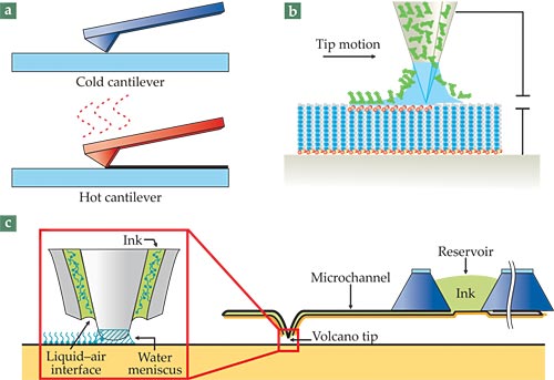
While modern-day Gutenbergs have invented nanoimprinting, others have reengineered the sixth-century quill pen on the nanoscale. Dip-pen nanolithography (DPN) uses an AFM with a nanocapillary to place atomic or molecular ink when and where it is wanted. 12 Some examples of how this truly impressive nanomanufacturing technology has been realized are shown in figure 4. The chemical compatibility of the source and substrate materials is critical, because the transfer of ink onto the substrate is sensitive to the local chemistry. For example, alkane thiolate inks (sulfur-terminated hydrocarbons) can be used to write on gold surfaces, and silanes (hydrogen–silicon compounds) can write on silicon. Solutions of metal salts in water can be used to deposit metals onto semiconductor surfaces.

Figure 4. Three examples of dip-pen nanolithography. (a) In thermal DPN, an atomic force microscope’s cantilever is coated with a solid ink that, when heated, liquefies and is deposited on the surface. (b) In electro-pen nanolithography, the tip simultaneously deposits the ink (green) and changes the surface chemistry to allow the ink to adhere to the surface. (c) In the nano fountain pen, a microchannel guides the ink from the reservoir to the tip, where it flows into the substrate though a water meniscus. (Adapted from ref.
With biomolecular inks containing proteins, DNA, or lipids, DPN is being used to build devices such as biosensors and nanoscale protein chips. Whereas other fabrication processes allow functionalization with biological markers and agents, DPN allows for the direct writing of biomolecules on soft matter and solid-state structures and even opens the possibility for direct writing onto or with living cells. The biocompatibility of the technique makes it a powerful tool for cell engineering, including stem-cell differentiation and subcellular drug delivery. Although throughput of a standard DPN setup is limited, two-dimensional arrays of thousands or even millions of tips have been used to massively speed up the process. 13 Such arrays could eventually help to mitigate one of the disadvantages of any AFM-based lithography system.
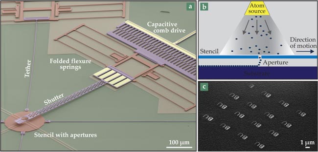
The last type of approach we will discuss is based on dynamic stencils. In the late 1970s, Gerald Dolan at Bell Labs showed how nanoscale features could be directly written using a static stencil as a shadow mask; a recent review highlights the subsequent developments in static stencil lithography. 14 Atoms or ions pass through the stencil apertures onto a substrate and thereby build nanostructures in the shape of the aperture pattern. Unlike resist masks, stencils can be used over and over.
A static stencil is limited to reproducing a previously defined pattern. Dynamic stencil lithography overcomes that limitation by allowing the stencil to move during the deposition. Figure 5 shows an example of a current-generation dynamic nanostencil setup for atomic calligraphy, or writing with atoms. Apertures tens of nanometers to 1000 nm in size are carved into a plate with a FIB. The plate is attached by four tethers to microelectromechanical linear motors that move it with subnanometer precision as atoms rain down onto the surface. The trajectory of the apertures results in a continuous trace of atoms deposited on the substrate below. Although the aperture defines a minimum feature size, or pixel, the path the aperture follows can be perfectly smooth. A shutter suspended over the plate stops and starts the passing of atoms and keeps unused apertures clean. Atoms can be dispensed in extremely small numbers, which gives a level of control suitable for fabricating monolayer circuits or controlled doping of existing structures. The plates can typically move at up to 0.1 m/s, considerably faster than conventional AFM tips, although throughput is currently limited not by the stencil speed but by the flux of atoms through the aperture. An array of apertures in a single plate can write repeating patterns quickly: With 10 000 50-nm apertures, throughput could reach 103 µm2/hr, comparable to that of e-beam or AFM methods.

Figure 5. Dynamic stencil lithography for atomic calligraphy. (a) A dynamic stencil with an integrated shutter. Both the stencil and the shutter are actuated using capacitive comb drives. The stencil is suspended over the substrate by tethers connected to folded flexure springs. (Adapted from M. Imboden et al., Nano. Lett.7, 3379, 2013, doi:
In our lab at Boston University, we are working on a project called “Fab on a Chip,” which will integrate nanoscale versions of all the tools of a modern foundry onto a silicon chip. 15 Material sources, mass sensors, and dynamic masks can all be integrated to form an on-chip assembly that enables rapid prototyping of nanoscale structures. The entire foundry will easily fit on a penny.
Future directions
Nanomanufacturing is an active and intense field of research. Many research groups around the world are aggressively pursuing the techniques we have discussed, and new technologies are being invented on a regular basis.
Many of the methods we have described are based on AFM technology, which currently suffers from low throughput. Work is being done to increase the scan speed using high-bandwidth mechanics 16 and by predistorting the drive for a step-and-settle response faster than the mechanical resonant frequency of the cantilevers would suggest. Another effort to increase throughput is by creating parallel arrays of AFM tips, which have already reached as many as 11 million tips for DPN systems.
To improve e-beam and FIB systems, faster beam-writing speeds using higher beam currents and more sensitive resists are the order of the day. In dynamic-stencil lithography, faster microelectromechanical plates, smaller apertures, and large arrays of apertures are where things are headed. In nanoimprint techniques, efforts are focusing on better dimensional stability and better overlay capabilities.
Nearly every area of applied physics and engineering is involved in some aspect of nanomanufacturing. Currently, each method fills a specific niche in which it bests other approaches. By leveraging the strengths of different technologies, researchers are developing processes that combine multiple techniques to write the highest-resolution masks that can be projected or printed with high accuracy and throughput. Clearly, the nanodevices of the future will be built by optimizing and combining the strengths of many technologies. There will never again be a one-size-fits-all approach, as optical lithography has been over the past four decades.
The worldwide semiconductor industry generates $300 billion in revenue annually. Its yearly R&D spending is $50 billion, much of which is focused on nanomanufacturing. Other industries, such as mass storage, telecommunications, cellular, and medical devices, also contribute R&D dollars. In comparison, to put a man on the Moon, the US Apollo program cost approximately $150 billion in 2014 dollars, or $15 billion per year. The investment being made in nanomanufacturing underlines the economic and strategic importance of the field. Although not generally recognized as such, nanomanufacturing is a major subfield of physics that engages large numbers of scientists around the world.
The intellectual challenges of moving from nanoscience to nanodevice-enabled products are daunting. Richard Feynman famously observed that “there’s plenty of room at the bottom”—but many researchers are working hard to make it a little more crowded.
We thank the NSF and its Civil, Mechanical, and Manufacturing Innovation Division for the ongoing support of our research.
References
1. G. E. Moore, “The Future of Integrated Electronics,” Fairchild Semiconductor internal publication (1964).
2. A. D. Franklin et al., Nano Lett. 12, 758 (2012). https://doi.org/10.1021/nl203701g
3. T. A. Brunner, J. Vac. Sci. Technol. B 21, 2632 (2003). https://doi.org/10.1116/1.1619954
4. D. M. Tennant, in Nanotechnology, G. Timp, ed., Springer (1999), p. 161.
5. X. N. Xie et al., Mater. Sci. Eng. R Rep. 54, 1 (2006). https://doi.org/10.1016/j.mser.2006.10.001
6. C. Gwyn et al., J. Vac. Sci. Technol. B 16, 3142 (1998). https://doi.org/10.1116/1.590453
7. W. Xiong et al., Light: Sci. Appl. 1, e6 (2012); https://doi.org/10.1038/lsa.2012.6
Z. Gan et al.Nat. Commun. 4, 2061 (2013).8. A. Grigorescu, C. Hagen, Nanotechnology 20, 292001 (2009). https://doi.org/10.1088/0957-4484/20/29/292001
9. P. Petric et al., J. Vac. Sci. Technol. B 27, 161 (2009). https://doi.org/10.1116/1.3054281
10. A. A. Tseng, Nano Today 6, 493 (2011). https://doi.org/10.1016/j.nantod.2011.08.003
11. N. Yao, Focused Ion Beam Systems: Basics and Applications, Cambridge U. Press (2007).
12. K. Salaita, Y. Wang, C. A. Mirkin, Nat. Nanotechnol. 2, 145 (2007). https://doi.org/10.1038/nnano.2007.39
13. D. J. Eichelsdoerfer et al., Nat. Protoc. 8, 2548 (2013).
14. O. Vazquez-Mena et al., Microelectron. Eng. (in press), doi:https://doi.org/10.1016/j.mee.2014.08.003 .
15. M. Imboden et al., Nanoscale 6, 5049 (2014). https://doi.org/10.1039/c3nr06087j
16. P. C. Paul et al., Nanotechnology 22, 275306 (2011). https://doi.org/10.1088/0957-4484/22/27/275306
17. J. A. Liddle, G. M. Gallatin, Nanoscale 3, 2679 (2011). https://doi.org/10.1039/c1nr10046g
18. G. M. Schmid et al., Proc. SPIE 7488, 748820 (2009).
More about the authors
Matthias Imboden is a postdoctoral associate in electrical and computer engineering, and David Bishop is head of the division of materials science and engineering and a professor in the departments of physics and electrical and computer engineering; both are at Boston University.


