The physics of boron nitride nanotubes
DOI: 10.1063/1.3518210
Tailored materials have long been central to condensed-matter physics. They often lead to new insights about the underlying physics governing the properties of materials—natural and synthetic—and sometimes provide new opportunities for applications. Superconductors are just one example. In the quest for higher transition temperatures, researchers have learned a great deal about superconductivity and the nature of electron-electron interactions. The goal usually pursued is “the higher, the better.”
In the case of nanoscience, however, the goal might be rephrased as “the smaller, the better.” Interesting physics invariably emerges as material dimensions approach the atomic scale and quantum size effects influence how electrons interact with each other (see the article by Michael Tringides, Mieczyslaw Jałochowski, and Ernst Bauer in Physics Today, April 2007, page 50 ). Dimensionality and symmetry restrictions also affect electronic behavior. When electron wavefunctions are confined to one or two dimensions, for example, the spectrum of collective excitations can change (see the article by Marc Kastner in Physics Today, January 1993, page 24 ), and properties that are familiar in bulk crystals can become unfamiliar in nanostructures.
Synthesizing intrinsically metastable nanostructures and characterizing them structurally, optically, thermally, electronically, or mechanically is challenging, but impressive advances in the field have been made. In addition to the usual atomic-scale microscopy techniques at their disposal, researchers have recently developed approaches for attaching individual wires or probes to isolated nanotubes and molecules for transport and mechanical measurements. Such approaches also probe molecular structures using methods—such as Raman spectroscopy, optical conductivity, and techniques that elicit a magnetic response—formerly amenable only to bulk materials.
The case of boron nitride nanotubes (BNNTs) is a good example of how theoretical and experimental research led to the discovery of a new material that has opened a path to exotic material properties, intriguing new phenomena, and unique applications. The 1994 prediction by one of our groups (Cohen’s) that BNNTs may exist 1 and a successful synthesis the following year 2 by the other (Zettl’s) gave credibility to the idea that calculation techniques developed for bulk solids should be applicable to nanoscale objects. Hence the standard theoretical models and tools work. Ever since, BNNT research has been active and is sure to grow considerably in the near future.
Carbon counterparts
Currently, the most widely studied nanostructures are based on carbon—carbon-60 buckyballs 3 and carbon nanotubes (CNTs) 4 are prime examples (see articles by Phaedon Avouris in Physics Today, January 2009, page 34 , and by Cees Dekker in Physics Today, May 1999, page 22 )—partly because its synthesis technologies are easily adaptable. Fortunately, interesting polyhedral and cylindrical structures are not limited to carbon, and the work of Reshef Tenne and his colleagues on transition-metal compounds has produced a variety of novel materials that are part of that class. 5 Indeed, numerous types of nanotubes and fullerene-like nanoparticles from inorganic layered (and even nonlayered) materials have emerged during the past two decades. The addition of BNNTs to the list—either in a pure form or in one that mixes C atoms into the composition, if desired—has given researchers yet another system to mine.
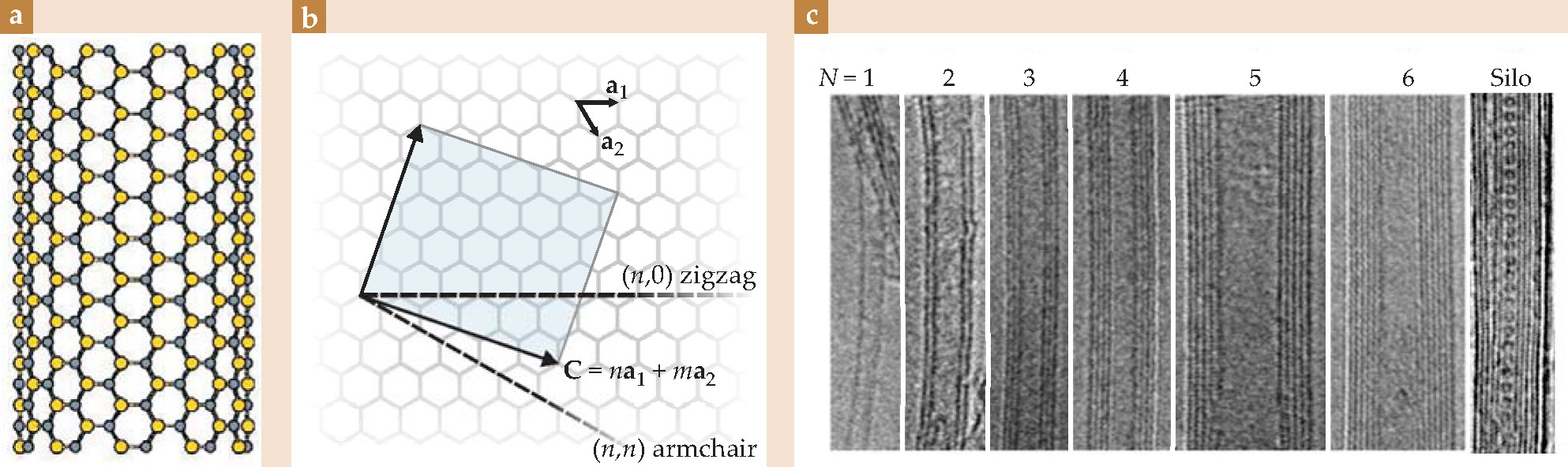
Structurally, BNNTs resemble CNTs: As sketched in figures 1(a) and

Figure 1. (a) A boron nitride nanotube (BNNT), shown schematically with its alternating boron and nitrogen atoms on a rolled hexagonal lattice. Certain synthesis methods create nanotubes that favor a so-called armchair orientation of atoms, as pictured here; others favor a zigzag orientation. (b) In terms of the unit vectors a 1 and a 2, a nanotube’s structural indices (n,m), the components of the circumferential vector C that circles the belly of a nanotube, indicate its orientation. Here, a nanotube whose orientation lies between armchair and zigzag is shown unrolled into a sheet whose area is given by the shaded square. (c) Nanotubes come in single-wall or multiwall forms—the nanotubes are single tubes or nested like Russian dolls. A set of transmission electron microscope images shows BNNTs whose wall numbers N span 1 to 6, with 3.4 Å being the interwall distance between nested tubes. The rightmost BNNT is filled with a linear chain of spherical carbon-60 molecules, constituting an elementary silocrystal.
On the other hand, h-BN is a purely synthetic material so far as anyone is aware, having been first synthesized in 1842. But its structural similarities to graphite have earned it the nickname “white graphite.” Tons of h-BN, widely used industrially as a high-temperature lubricant, are produced each year. Beyond its electronic bandgap and striking white color, many of the material’s properties are also found in BNNTs, including thermal stability at extreme temperatures in oxidizing environments and an ability to absorb neutron radiation.
Despite the relative ease and low cost of industrial-level h-BN production, identifying an efficient production route for BNNTs has been difficult. This is perhaps understandable in that h-BN, not the BNNT, is the lowest-energy form of BN, just as graphite is the lowest-energy form of carbon. Higher-energy forms of carbon, such as diamond, fullerenes, or nanotubes, are metastable and rare in nature. Other allotropes of BN, in particular those with curvature, are metastable as well. That does not imply, however, that BNNTs are intrinsically unstable. In fact, relative to their planar parent structures, BNNTs are more stable than CNTs. 6 Once formed, BNNTs are rather difficult to destroy, chemically or thermally.
Synthesis
The first BNNTs were synthesized by introducing h-BN into the high-temperature plasma formed between two arcing tungsten electrodes.
2
That process yielded high-quality tubes, but in limited quantities and with little control over tube diameter, chirality (that is, handedness), or wall number—the number of nanotubes that nest within each other. Figure
Fortunately, those geometrical variations are less important to BNNTs’ electronic properties than they are to CNTs’: All of the BNNTs in the first six panels of Figure
Many methods have been used to produce BNNTs, including laser vaporization; chemical vapor deposition, which relies on cooler, easier-to-control plasmas; the “templated conversion” of C-containing nanotubes, in which B and N atoms replace the C framework atom by atom; plasma spraying, in which raw materials that eventually make up the BNNT are sprayed through the hot ionized gas; and even crude ball milling and annealing of BN powders. 8 Importantly, h-BN is not a necessary precursor to the successful production of BNNTs. Virtually any boron-containing material, including pure boron, can be suitably reacted with a readily available nitrogen source, such as N2 gas or ammonia, to grow BNNTs. A particularly effective recent production method focuses kilowatt-power laser beams on boron-containing feedstock in a high-pressure nitrogen atmosphere. 9 The development of that and other high-throughput synthesis methods is yielding larger quantities of samples and rapidly changing the landscape of BNNT scientific study.
Predicting properties
Although limited access to BNNT materials hampered experimental studies in the past, theoretical research has been relatively active. Tight-binding models, pseudopotential total-energy methods within the local-density approximation, and quasiparticle extensions of density functional theory were all used to study and predict the structural and electronic properties of BNNTs. Further theoretical calculations predicted that the ionic nature of the BN bond would cause a buckling of the tube surface, with the N atoms forming a slightly larger cylinder than the B atoms.
That asymmetry may be involved in the shell-shell stacking structure of multiwall BNNTs. As mentioned earlier, N and B atoms in h-BN prefer to stack directly over one another in adjacent sheets. Indeed, high-resolution microscopy and diffraction studies reveal that strong correlations exist between BNNT shells, each inner shell matching the outer ones in chirality. 8 (In CNTs, by contrast, little structural correlations exist between shells, and the chiralities of shells nested in a multiwall CNT are generally random.)
Certain BNNT synthesis methods also appear to favor the production of so-called zigzag-type shells, while others favor armchair-type shells (see figure 1(a)). That is, it’s now possible for researchers to subtly modify their synthesis recipe to select particular chiralities when making a batch of BNNTs. In double-wall tubes grown using an arc plasma, for instance, the first-formed inner shell tends to be zigzag.
The structural correlations between nested shells are likely to have important implications for mechanical and thermal transport properties and to have ramifications for how easily the tubes can bind to other molecules, so-called functional groups. Moreover, BNNTs may be more resistant to structural defects. In the case of C-based structures, pentagonal and heptagonal defects are prevalent; they are, after all, at the heart of icosahedral symmetry in closed fullerenes.
In BN planar structures, analogous defects would necessitate B-B or N-N bonding, either of which is less favorable than B-N bonding. One could even argue that given suitable feedstock and typical synthesis conditions, BNNTs are less likely than CNTs to stop growing due to capping. And most pristine multiwall BNNTs do appear uncapped when examined by transmission electron microscopy. The lowest-energy defects in BNNTs are even-numbered rings such as squares or octagons.
The polar nature of the BN bond also led to the theoretical prediction that in contrast to CNTs, BNNTs would consistently be semiconductors irrespective of their differing diameters and chiralities. 10 Researchers therefore don’t face the problem encountered in a batch of CNTs—separating metallic nanotubes from semiconducting ones; both can form depending on how the CNT is rolled up. According to calculations, the BNNT bandgap is close to 5 eV, which makes the material relevant for a wide range of optical studies. A plot of the band structure is shown in figure 2. A local density approximation underestimates the BNNT bandgap, as it does for other semiconductors and insulators, but approaches that correct for the many-body interactions give reliable results.

Figure 2. The calculated electronic band structure of a boron nitride nanotube (BNNT) exhibits an approximately 5-eV gap between its highest filled valence band and lowest empty conduction band. That bandgap is relatively independent of tube diameter and chirality, meaning that all BNNTs are similar electronically and behave like wide-gap semiconductors. The lowest conduction band (red) exhibits parabolic dispersion and is thus free-electron-like. Remarkably, charge carriers introduced into that lowest conduction band, either by doping or by direct injection, reside not on the tube but inside it, concentrated in the hollow center along the BNNT axis, as suggested in the schematic. (Adapted from refs. 1 and 10.)
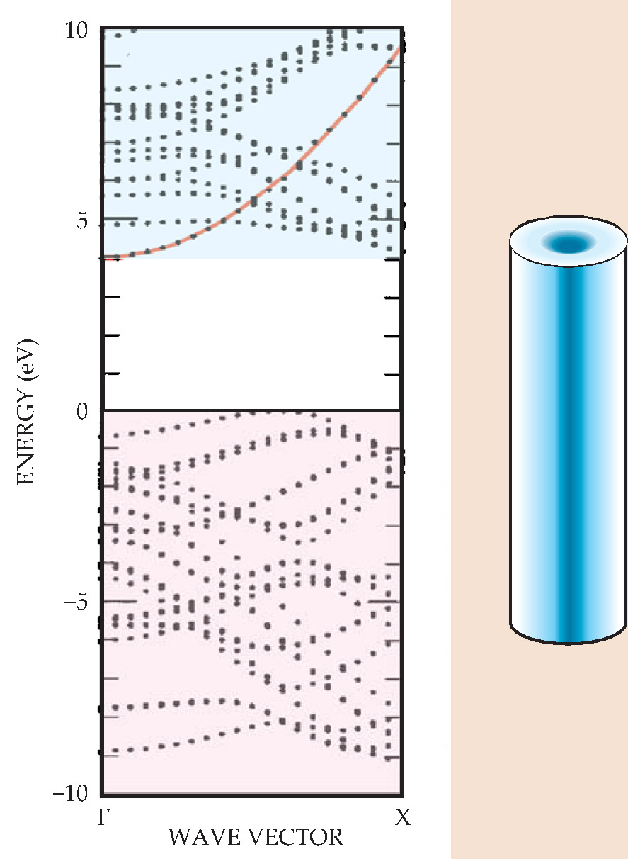
Doping BNNTs with impurities, either within the tube wall or via functionalization — chemically modifying the nanotubes so that external molecules may bond to them—can change the electronic properties considerably, just as for common semiconductors. But BNNTs present some interesting twists that set them apart from traditional semiconducting materials. One unusual feature is that the charge density associated with a BNNT’s lowest conduction band is physically concentrated in the tube’s interior. If doped with electrons, the charge resides inside the tube, not on it, with a charge-density maximum about 2 Å inside the wall. Therefore, the doped nanotubes tend to act like pipes filled with virtually free electrons, as shown schematically in figure 2.
It’s also possible that charges injected into the ends of an undoped or only slightly doped BNNT could occupy that special, lowest conduction state, leading to highly non-ohmic electronic conduction. Indeed, the current-voltage characteristics of lightly doped individual BNNTs show that at a threshold applied voltage of around 10 V, conduction rises sharply. 11
Furthermore, lightly doped BNNTs are excellent electron field-emission sources, with emission turn-on voltages comparable to those of CNTs. In contrast to CNT field emitters, though, the BNNT field emitters exhibit currents that are extremely stable and closely follow what’s known as the Fowler-Nordheim law for tunneling emission. Stable field-emission sources are critical to various high-resolution microscopies, x-ray generation, and low-power display technologies.
Tuning the gap
Another interesting theoretical prediction is that the BNNT bandgap, thanks to the nanotubes’ low dimensionality and cylindrical geometry, can be externally and reversibly tuned after the material has been produced. Because the conduction and valence bands have degeneracies at the band edges, and because there’s little screening of free charges, the gap between the bands is particularly sensitive to a transversely applied electric field. Theory predicts that the bandgap can be reduced and, provided the applied field is strong enough, even eliminated, 12 as shown in figure 3. That giant Stark effect is analogous to the conventional Stark effect found for atomic orbitals.

Figure 3. An electric field applied transverse to the boron nitride nanotube axis breaks some of the degeneracies in the material’s band structure. As the field increases, the bandgap progressively narrows; that property can be exploited to tune the electronic behavior. (a) Calculations show that nanotubes with larger diameter d are more sensitive to the effect, and at sufficiently high field the conduction and valence bands merge, which can make the nanotubes metallic. (b) At a transverse field of E = 0.1 V/Å electrons become concentrated on one side of the nanotube (top), while holes pile up on the other (bottom). (Adapted from ref. 12.)
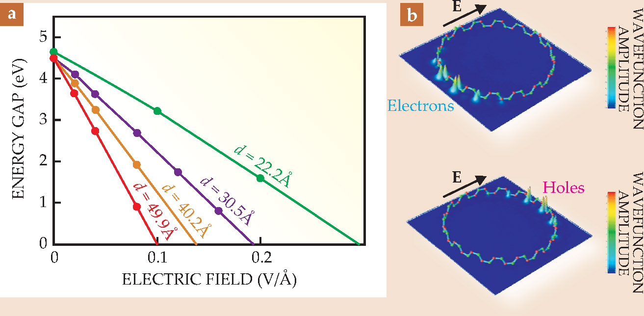
The mixing of electronic states in a BNNT in a transverse electric field is enhanced because of the field-induced splitting of the electronic bands. The reduced screening, because of the insulating behavior, allows the field to set up a significant difference in electric potential between opposite sides of the tube. And states with similar wavefunctions that would be degenerate at opposite sides of a tube in the absence of a field become split. Consequently, electrons and holes accumulate on opposite sides of the BNNT.
Researchers have confirmed the giant Stark effect using the tip of a scanning tunneling microscope (STM) to impose a strong local electric field on a BNNT. 13 And the local field-modified gap was determined by STM spectroscopy. Therefore, not only can the electronic structure of BNNTs be changed through doping, but theoretical and, to a lesser extent, experimental studies suggest that the bandgap can be continuously tuned from nearly insulating to effectively metallic behavior. A similar effect also occurs in CNTs but is not nearly as pronounced as in BNNTs.
Another manifestation of the reduced dimensionality and confinement of electrons in nanotubes (both CNTs and BNNTs) shows up in the materials’ optical properties, which exhibit unusual excitonic effects. In metallic CNTs, excitons, which are pairs of electrons and holes bound together by their mutual Coulomb attraction, shouldn’t be able to exist: A free electron would recombine with its hole almost immediately after an exciton formed. And yet they do exist, with a binding energy greater than that of the excitons in most bulk semiconductors. 14 Researchers have only begun to explore the optical properties of BNNTs. They appear to be similar to those of CNTs, but with a richer spectrum because of the BNNTs’ reduced electron screening.
Applications and speculations
Boron nitride nanotubes provide a versatile platform for additional novel physics phenomena and applications. Figure 4 outlines just a few of the different contexts in which BNNTs are being explored. BNNTs can be spun into white yarns and dyeable textiles. A field-tunable bandgap has obvious implications for optical and electronic devices. The material’s high surface area and ability to bond to hydrogen and other molecules could put it in the service of clean and efficient fuel storage. Its high stiffness and tensile strength, along with its rich functionalization chemistry (one example is illustrated in figure 5), could be employed in structural composites and energy-absorbing protective devices. BNNTs are also piezoelectric.

Figure 5. Nano Velcro. The surface of boron nitride nanotubes (BNNTs) can be chemically modified to accept a variety of molecular linkers, including those that facilitate binding to selected nanocrystals or biomaterials. Such modifications yield intriguing systems whose optical and electronic-transport properties and chemical reactivity can be tailored. In this illustration, short-chain alkanes with a terminal sulfur atom are attached to the BNNTs.
(Image courtesy of Toby Sainsbury.)
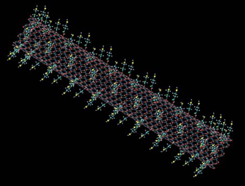

Figure 4. A gallery of nanotubes. Boron nitride nanotubes (BNNTs) find application in a wide range of contexts. (a) (Adapted from ref. 9.) They can be wound into white, dyeable fibers and superstrong composites. (b) (Adapted from ref. 18.) They can also be exploited for their high thermal conductivity, a property that has been measured for single BNNTs, as shown in this electron micrograph of a nanotube spanning two ends of a micromechanical heat source; the inset contrast is reversed for clarity and its orientation inverted. (c) Molecules can be embedded within the nanotubes, like peas in a pod. These filled nanotubes, known as silocrystals, can be synthesized into a variety of exotic forms potentially useful for quantum computation, field emission, or applications that require specifically tailored optical properties. (d) Alternatively, molecules can be attached outside the nanotube, for use, say, in catalysis, chemical filtering, or storage of gases. This electron micrograph shows gold clusters on a BNNT.
For high-temperature oxidation resistance, BNNTs have no equal. Their ability to bond with other nanocrystals also suggests they may be used as harsh-environment catalysts, water purification systems, plasmonic devices, and photovoltaics. With boron’s high neutron-absorption cross section, radiation-hardened BNNT-based composites may be viable materials for aircraft and space exploration. They have even been suggested for neutron-based cancer treatment, in which cancer cells that have injested BNNTs are preferentially heated via neutron absorption of 10B.
An important issue for nanomaterials of all kinds is bio-compatibility. Early nanomaterials studies focused mainly on the effects of having needlelike structures puncturing cells and organs. The effects are complex and size dependent. Recently, more sophisticated experiments have explored the interaction of nanomaterials with biosystems, and some carbon nanomaterials, including CNTs, have been shown to damage living cells. Under similar conditions, BNNTs appear to have no such adverse effect. 15
The BNNTs can also be functionalized with biological epitopes—the parts of an antigen that mediate protein and cell binding—and BNNTs have been used with no apparent toxicity to deliver DNA oligomers to the interior of cells. 15 BNNTs’ very high thermal conductivity, with no electrical conductivity, has implications for general thermal management in any number of systems.
Ordering atoms around
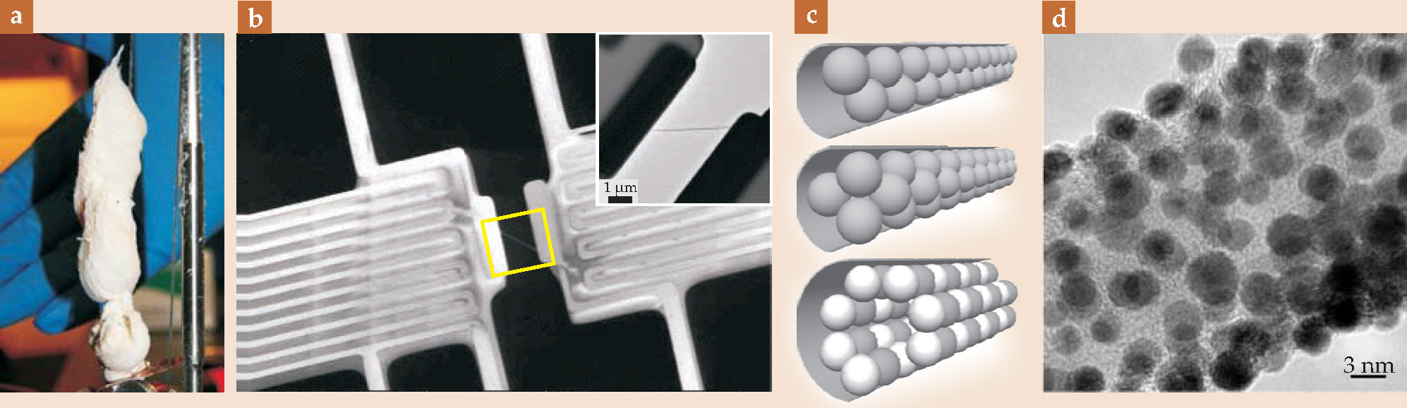
New physics often arises from new materials formed out of unique combinations of elements—examples include oxide superconductors, quasicrystals, giant-magnetoresistance systems, and topological insulators—or from external constraints, such as a high magnetic field or high pressure placed on relatively inert materials. One type of constraint only recently explored is that of nanoscale cylindrical confinement. When the nanotubes’ diameter is small, a linear chain of C60 molecules can be squeezed into them, creating what are known as silocrystals, as shown in figure
Molecules organize linearly in the tubes not because of intermolecular forces but because the narrow cylinder closely matches their diameter. When the same molecules are confined within larger-diameter cylinders, novel structures emerge, such as the staggered linear chain and spiral structures sketched in figure
BNNTs are the ideal host for a C60 silocrystal because they interact little with the molecules, and the large electronic bandgap of BNNTs allows researchers to optically probe the silocrystal. Furthermore, because BNNT shells themselves are electrically insulating, electrical charge is transported through the silocrystal. Such systems are just beginning to be explored theoretically and experimentally, but the scientific opportunities appear large, especially since many different materials are easily encapsulated within BNNTs. 8
The relatively defect-free nature of BNNTs sets the stage for a variety of mechanical and atomic vibrational studies. Indeed, the axial Young’s modulus, measured at 1.2 TPa, is the highest of any insulating fiber.
Isotope substitutions have played key roles in some of the most important problems of condensed-matter physics, including the theory of superconductivity. Since phonons contribute to the thermal properties of solids, the thermal conductivity k T of solids can also often be influenced by isotopic content. Room-temperature k T enhancements of 10-30% have been achieved in silicon and germanium, and of up to 35% in diamond via isotopic enrichment.
Even without isotopic enrichment, BNNTs are excellent heat conductors, and they spectacularly exhibit the largest enhancement of k T by isotopic substitution of any material. The boron isotopic content of BNNTs grown from natural materials is 19.9% 10B and 80.1% 11B. For BNNTs enriched to 99.56% 11B, k T at room temperature is enhanced by 50%. 18 That dramatic isotope-enhancement factor likely has sources beyond the usual phonon-impurity scattering mechanism. The 1D structure of BNNTs should increase the enhancement factor by promoting phonon localization and additional scattering events that favor light atoms.
Finally, a few comments are in order concerning the planar form of sp 2-bonded BN in single or few-layer sheets. The current surge in research on graphene and its relationship to CNTs raises the question of whether a similar surge will develop as researchers explore the connections between BNNTs and h-BN sheets. It is probably safe to predict that it will. It’s also likely that if BN ribbons are made, their physical properties should be even more varied than those predicted for graphene. Not only will structures with reproducible armchair and zigzag edges possibly exist, but the two-element nature of the edges should greatly influence the structures’ electronic and magnetic properties.
As we’ve tried to emphasize in this article, BNNTs offer so much potential themselves—independent of activity on BN sheets—that basic and applied research focusing on their own physics and chemistry is likely to remain a source of excitement and become a large enterprise.
The authors acknowledge support by the US Department of Energy, Office of Basic Energy Sciences, under contract DEAC02-05CH11231, and by NSF under grants DMR07-05941 (MLC) and EEC-0832819 (AZ).
References
1. A. Rubio, J. Corkill, M. L. Cohen, Phys. Rev. B 49, 5081 (1994). https://doi.org/10.1103/PhysRevB.49.5081
2. N. G. Chopra, et al., Science 269, 966 (1995). https://doi.org/10.1126/science.269.5226.966
3. H. W. Kroto, et al., Nature 318, 162 (1985). https://doi.org/10.1038/318162a0
4. S. Iijima, Nature 354, 56 (1991). https://doi.org/10.1038/354056a0
5. R. Tenne, et al., Nature 360, 444 (1992). https://doi.org/10.1038/360444a0
6. Y. Miyamoto, et al., Phys. Rev. B 50, 4976 (1994). https://doi.org/10.1103/PhysRevB.50.4976
7. A. Loiseau, et al., Phys. Rev. Lett. 76, 4737 (1996). https://doi.org/10.1103/PhysRevLett.76.4737
8. D. Golberg, et al., Adv. Mater. 19, 2413 (2007), and references therein. https://doi.org/10.1002/adma.200700179
9. M. W. Smith, et al., Nanotechnology 20, 505604 (2009). https://doi.org/10.1088/0957-4484/20/50/505604
10. X. Blase, et al., Europhys. Lett. 28, 335 (1994). https://doi.org/10.1209/0295-5075/28/5/007
11. J. Cumings, A. Zettl, Solid State Commun. 129, 661 (2004). https://doi.org/10.1016/j.ssc.2003.11.026
12. K. H. Khoo, M. S. C. Mazzoni, S. G. Louie, Phys. Rev. B 69, 201401 (2004). https://doi.org/10.1103/PhysRevB.69.201401
13. M. Ishigami, et al., Phys. Rev. Lett. 94, 056804 (2005). https://doi.org/10.1103/PhysRevLett.94.056804
14. F. Wang, et al., Phys. Rev. Lett. 99, 227401 (2007). https://doi.org/10.1103/PhysRevLett.99.227401
15. X. Chen, et al., J. Am. Chem. Soc. 131, 890 (2009). https://doi.org/10.1021/ja807334b
16. B. W. Smith, M. Monthioux, D. E. Luzzi, Nature 396, 323 (1998). https://doi.org/10.1038/24521
17. W. Mickelson, et al., Science 300, 467 (2003). https://doi.org/10.1126/science.1082346
18. C. W. Chang, et al., Phys. Rev. Lett. 97, 085901 (2006). https://doi.org/10.1103/PhysRevLett.97.085901
More about the authors
Marvin Cohen and Alex Zettl are professors of physics at the University of California, Berkeley, and senior faculty scientists at Lawrence Berkeley National Laboratory. Zettl also directs the University of California’s Center of Integrated Nanomechanical Systems.
Marvin L. Cohen, University of California, Berkeley, US .
Alex Zettl, University of California, Berkeley, US .


