The graphene–semiconductor Schottky junction
DOI: 10.1063/PT.3.3298


A single plane of carbon atoms arranged in a honeycomb lattice, graphene was isolated in 2004 with the now-famous Scotch-tape method: University of Manchester physicists Andre Geim, Konstantin Novoselov, and their colleagues peeled away weakly bound layers from bulk graphite with the tape and then gently rubbed those layers onto an oxidized silicon surface. More significantly, they prescribed how to locate with an optical microscope the rare graphene flakes among the multilayer graphite debris. 1
Graphene wasn’t new at the time. Organic chemist Hanns-Peter Boehm had synthesized it from graphite oxide in solution nearly half a century earlier, in 1962, and Philip Wallace had calculated its band structure 15 years before that. But through their simple, cheap, and quick method for making high-quality, device-ready crystals, Geim and Novoselov sparked an explosion of experimental and theoretical graphene research. It immediately became possible not only to study the two-dimensional material but also to control its fabrication and integration into devices. (See Physics Today, December 2010, page 14 , and the article by Geim and Allan MacDonald, Physics Today, August 2007, page 35 .)
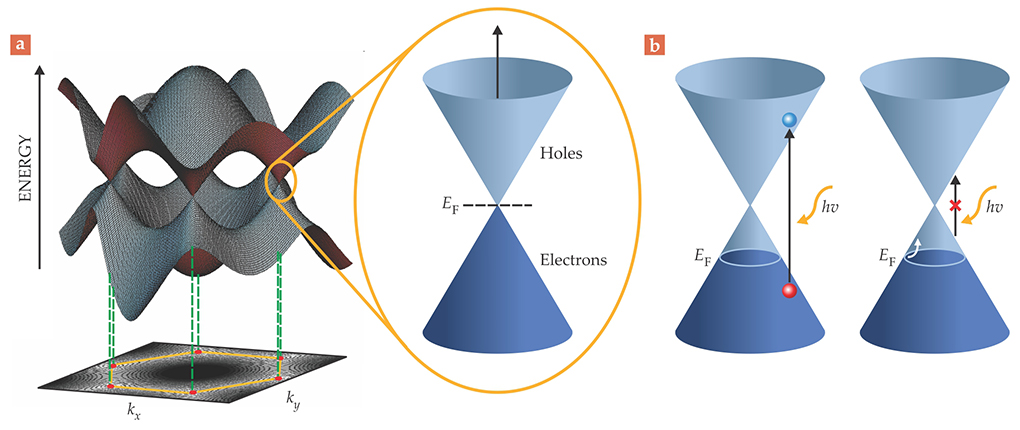
The appeal of device integration stems from graphene’s advantageous properties. The material boasts an electron mobility exceeding 10 000 cm2/Vs when deposited on SiO2 or Si—that’s an order of magnitude higher than the mobility in Si. And because of the gapless nature of its band structure, pictured in figure 1, graphene can absorb light across a broad spectrum—from the UV to IR wavelengths. Along with those electronic and optical properties, the material is mechanically strong, elastic, chemically stable, and thermally conductive.

Figure 1. Graphene’s band structure. (a) Graphene, a semimetal, has linearly dispersive valence and conduction bands that meet at discrete points in its momentum-space representation. In the pure crystal, the Fermi level EF, or chemical potential, is at those points. (Courtesy of Philip Kim.) (b) If graphene is doped, however, the Fermi level can rise or fall. And if the incident light is high enough in energy hν to induce interband transitions, then 2.3% of that light is absorbed by the crystal. The absorption promotes an electron (blue) to the conduction band, which leaves a hole (red) behind. If the light energy is too low, only intraband transitions (white arrow) in the valence band can occur.
What’s more, every atom resides on graphene’s surface. The material thus offers the largest possible contact area with its environment, which makes it an ideal platform for sensing applications. Because of the atomic thinness of graphene, though, its interaction with the supporting substrate is critical to its performance in devices. Few researchers use Scotch-tape exfoliation of graphite to mine their graphene anymore. Fortunately, graphene is compatible with standard thin-film processing techniques used in the electronics industry, and the material can be grown epitaxially by thermal decomposition of silicon carbide or by chemical vapor deposition (CVD) of hydrocarbons on a surface.
In this article we discuss one of the simplest building blocks for graphene-based electronics: a layer of graphene atop a semiconductor, whose contact forms a so-called Schottky junction. For a more comprehensive treatment, see references and .
Device building block
Metal–semiconductor contacts, p–n junctions, and metal-insulator-semiconductor structures are the basic components of most electronic devices. Since 1874, when Ferdinand Braun probed a lead sulfide crystal with the point of a metal wire and discovered the free flow of current in only one direction, researchers have studied the intimate contact between metals and semiconductors. But a basic theory behind the rectification behavior emerged only decades later when Walter Schottky and other innovators realized that a potential barrier, now known as a Schottky barrier, exists across the junction.
Two kinds of devices are produced by the metal–semiconductor contact: the ohmic junction, in which the ratio between current and voltage follows Ohm’s law and is typically made from highly doped semiconductors; and the Schottky junction, which is typically made from lightly doped semiconductors and behaves like a diode, with high current and low resistance in one direction and negligible current and high resistance in the other.
To appreciate what produces the rectification, keep in mind that the Fermi level EF, or chemical potential (for a metal, the highest energy state electrons occupy at zero temperature), can differ in a metal and a semiconductor. That means that the work function—the energy required to pull an electron from a solid—of each also differs, and on contact with each other the disparity in their work functions causes electrons to flow from one to the other until their Fermi levels align. In addition, the charge transfer depletes a region of free charges just inside the semiconductor interface. In the case of n-type semiconductors, the removal of electrons in that depletion layer leaves behind immobile positive charges that cause the semiconductor’s valence and conduction bands to bend upward at the interface. At equilibrium, when the Fermi levels have aligned, the discontinuity in allowed energy states of the two materials produces the Schottky barrier, which blocks the flow of electrons from the metal to the semiconductor.
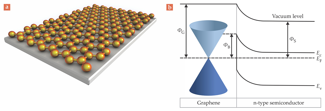
That conventional model of metal–semiconductor contacts is the basis for our understanding of the graphene–semiconductor Schottky junction shown in figure 2. But whereas in the conventional model, the Fermi level of the metal stays constant because of the metal’s high density of states, the Fermi level of graphene may be sensitively tuned by applying an appropriate bias voltage or by chemically doping the material with impurities. 4 Shining light on graphene, which can promote electrons from its valence band to its conduction band (as outlined in figure 1b), can further affect the material’s charge density and the position of the Fermi level. 5 That controllability is important because the Schottky barrier height of the junction mainly depends on graphene’s Fermi level.

Figure 2. A Schottky junction refers to the intimate contact formed between two materials—(a) here, graphene (gold) atop an n-doped semiconductor (gray)—that produces an electric field and one-directional current flow from one material to the other. (b) In this representative energy-band diagram of the graphene–semiconductor Schottky junction, ΦG and ΦS are graphene and semiconductor work functions—the energy difference between the vacuum level (the energy of an electron outside the material) and the Fermi level EF. EC and EV represent the semiconductor’s conduction-band minimum and valence-band maximum, and ΦB is the Schottky barrier height, the energy barrier to electrical conduction across the junction. When contact is first established, and assuming that ΦG > ΦS, electrons will flow from the semiconductor to graphene and bend the bands in order to align Fermi levels; electrons flow in the opposite direction in p-type semiconductors.
Those controls and researchers’ ability to manipulate them make graphene a valuable component for optoelectronic devices. Currently, various semiconducting materials, including traditional 3D organics and inorganics, 2D layered semiconductors, 1D nanostructures, and 0D quantum dots, are used to create Schottky junctions with graphene. The junctions they make form the basis for solar cells, photodetectors, lasers, LEDs, chemical sensors, and more, and they are the building blocks for other, more complex graphene-based devices.
A little history
The history of research on carbon–semiconductor contacts dates back to a century ago, although the earliest studies revealed few significant discoveries because the technologies of materials preparation and device fabrication were in their infancy. As early as 1914, Ralph Hartsough at the University of Kansas found a pronounced rectification when he abutted C (mostly likely in the form of graphite) and Si to form a point contact.
6
In 1962, during subsequent research on electrode contacts on semiconductors, George Harman and Theodore Higier from the National Bureau of Standards (now NIST) found that graphite electrodes on p-type Si behaved as ohmic contacts.
7
But the study of carbon–semiconductor junctions suffered from long periods of neglect during the 20th century (see the box on page
Even so, only within the past few years have graphene-based Schottky junctions been investigated systematically. In 2009 Filippo Giannazzo of the National Research Council in Catania, Italy, and his colleagues prepared the first Schottky junction between graphene and SiC and measured its barrier height using scanning current spectroscopy. 8 The following year, the two of us and our colleagues prepared a graphene-on-silicon Schottky junction using chemical vapor deposition and successfully demonstrated rectification characteristics and photovoltaic performance. 9
Light detection
Because graphene’s Fermi level is tunable, so are its optical properties. Graphene’s ultra-broadband response to light and its high carrier mobility make the graphene–semiconductor junction an ideal photodetector. 10 The device, which can be modeled as a photodiode, is highly sensitive, responds to input light quickly, and detects even faint signals with a minimum of noise. The basic operation is to separate photo-generated electron–hole pairs and collect them in different parts of a circuit with an electric field.
A graphene-based photodetector can work in different modes, as outlined in figure 3. When the incident photon energy is high, electron–hole pairs are predominantly produced in the depletion layer of the semiconductor. In that mode, the quantum efficiency, or number of charge carriers generated per photon, can be tailored by adjusting the thickness of the layer. Unlike metals, which reflect much of the light, graphene allows nearly 98% of it to pass through into the semiconductor. One can introduce an interfacial layer, typically an oxide, between graphene and the semiconductor to enlarge the barrier height. The enlargement reduces the junction’s dark, or unwanted, current in the absence of incident light and thus improves the signal-to-noise ratio. 11

Figure 3. A graphene–semiconductor photodetector can work in two main modes. Imagine a Schottky junction formed between the two materials and a voltage bias applied to the graphene with respect to the semiconductor. (a) When the incident photon energy hν exceeds the semiconductor bandgap Eg, electron–hole pairs (blue and red) are generated in the semiconductor’s depletion layer (orange), a region depleted of electrons just inside the semiconductor’s surface. (b) When the Schottky barrier height ΦB (see figure
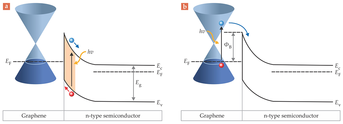
Another mode, known as internal photoemission, is useful at long wavelengths, such as the IR, a part of the spectrum to which many semiconductors are insensitive at room temperature. 10 Although the photons are too weak to excite electrons above the semiconductor’s bandgap, they can generate electron–hole pairs in graphene, whose Fermi level can be tuned so that electrons surmount the Schottky barrier height. The charge carriers then pass from graphene into the semiconductor and contribute to the current.
Solar cells
Solar cells are a type of photodiode designed purely for power output. Although Si-based solar cells have made great progress since their debut decades ago as simple p–n junctions (see the article by Jack Stone, Physics Today, September 1993, page 22 ), three key issues remain: improving performance, reducing the amount of materials, and simplifying the manufacturing process. As a single atomic layer of material with exceptional properties, graphene can ameliorate all three concerns.
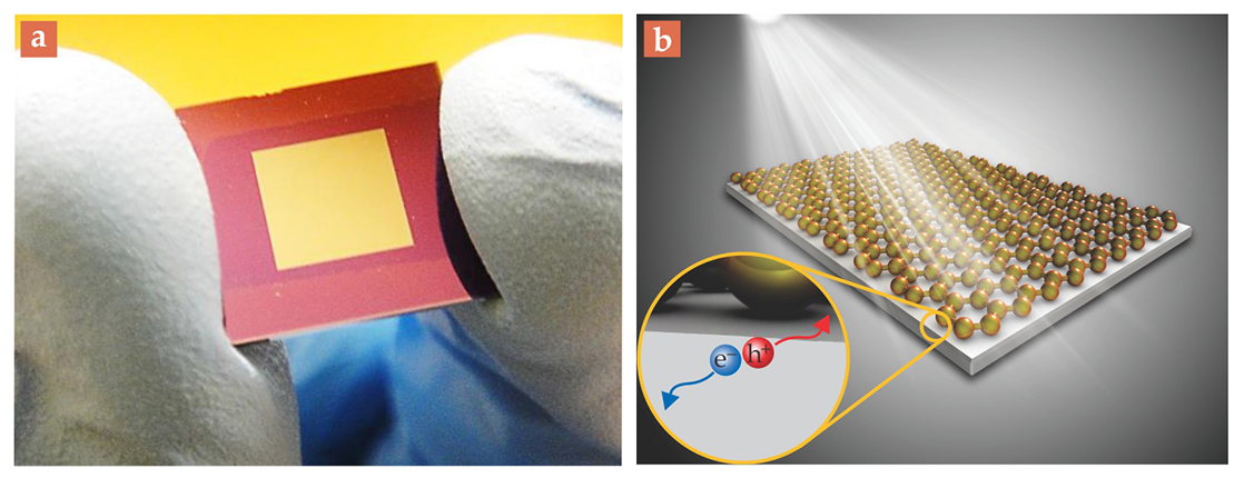
Even so, in 2010 when we fashioned our first graphene–Si Schottky junction, 9 shown in figure 4a, we found that it performed only modestly as a photovoltaic device. Its peak power-conversion efficiency (PCE), the ratio of output electrical power to incident solar radiation power, was just 1.7%. In our simple configuration, graphene served not only as a transparent electrode but also as the active layer atop Si for electron–hole separation. Because of the intrinsic electric field created at the Schottky junction, electrons migrated into the Si and holes migrated in the opposite direction, as shown in figure 4b. And with its modest refraction index, the CVD-prepared graphene electrode provided an antireflection effect.

Figure 4. The graphene– semiconductor solar cell. (a) A 2011 photograph of a rudimentary graphene–silicon solar cell, about 2 cm across. Not shown are an antireflection coating and metal contacts for connecting it to a circuit. (b) When the graphene–Si Schottky junction (the interior gold square in the photograph) is exposed to sunlight, photo-induced charge carriers—electrons (e−) and holes (h+)—are mainly generated in the semiconductor and are separated by the built-in potential created by the junction.
Since then we have improved our methods for doping graphene and tying up dangling bonds on the Si surface to make it chemically inert to the C, which produces a more stable junction. Those and other improvements increased the PCE of our graphene–Si solar cells to 15.6%, the highest efficiency reported to date 3 for a graphene–Si solar cell and on par with the 15–20% efficiency of most commercial Si cells.
To reach that near-16% efficiency, the challenge was to maximize the collection of light in the cell and minimize the recombination of electron–hole pairs throughout it. For the latter, doping graphene with acids, organic molecules, implanted ions, or liquid electrolytes turned out to be effective approaches. Those chemical doping methods not only improve graphene’s conductivity, they also allow graphene’s Fermi level to be optimally tuned to maximize the internal potential of the graphene–Si Schottky junction. The internal potential, and thus maximum open-circuit voltage—defined by setting the current in the junction to zero—can also be increased by inserting an interfacial layer, as described above. 11
Because graphene is atomically thin and highly transparent, the incident light is absorbed in Si’s depletion layer. But to maximize the amount of light penetrating the semiconductor, it’s necessary to add an antireflection coating to the shiny, reflective graphene–Si interface. In recent work, researchers have incorporated common antireflective materials, such as titanium dioxide, into their solar cells. The next challenge is to design a more efficient light-trapping scheme for various wavelengths and incident angles of sunlight.
The work done so far on graphene–Si solar cells is just a start. Researchers are already making solar cells out of graphene deposited atop other semiconductor materials, such as III–V compounds, II–VI compounds, ternary compounds, perovskites, and organic semiconductors.
The bulk and the atomic
The story of the graphene–semiconductor junction is likewise not over. Experimentalists continue to strive to create the ideal Schottky junction by reducing the number of atomic defects and charge-trapping sites it contains. And although the junction’s atomic structure influences the behavior of the Schottky barrier, the classical model of its effect is based on bulk 3D material. Theorists are working on modified models that are applicable to the interface between a single atomic layer and a semiconducting material.
The physics becomes even richer for systems whose behavior is governed by more than a single interface. The multilayer van der Waals heterojunctions formed by stacking graphene and other 2D materials, such as boron nitride and molybdenum disulfide, offer opportunities for theorists and experimentalists to construct and study the principles by which atomic-layer devices work. 12 For that story, turn to the article by Pulickel Ajayan, Philip Kim, and Kaustav Banerjee on page 38 of this issue.
Box. The carbon–silicon junction
Silicon is the most thoroughly studied and widely applied semiconductor material in the electronics industry. The raw material is cheap, abundant, and can be fabricated into devices using techniques that have benefited from decades of refinement. Carbon, another abundant material, shares a similar electronic structure: Like Si, C contains four electrons in its outer orbital, and the two elements reside in the same column of the periodic table. But in stark contrast with its neighbor, C can form a variety of stable allotropes, each with different electronic and mechanical properties that depend on the type of bonding—sp, sp2, or sp3—the atoms experience.
The most common forms of crystalline carbon are graphite, whose planes of sp2-bonded C atoms are arranged in a honeycomb lattice, and diamond, whose atoms have sp3 bonding. In the diamond lattice, the structure also shared by Si, all four electrons form strong covalent bonds between atoms.
With the development of increasingly sophisticated materials-production techniques beginning in the 1970s, new C allotropes emerged. Diamond-like C thin films, an amorphous form of C containing a fraction of sp3 bonds, were prepared in 1971 using ion-beam deposition. In 1985, molecules of C60, known as fullerenes, were discovered; in 1991, carbon nanotubes were identified in the soot from a C arc discharge; and in 2004, graphene was rescued from relative obscurity by a technique that made it easy to isolate. 1 Each of the new allotropes rekindled an enthusiasm for C-based technologies with applications for both fundamental science and commercial devices.
Researchers began appreciating the value of C–Si junctions for electronics in the late 1970s, when C films could be controllably fabricated along with other materials such as metal electrodes and semiconductor substrates. In 1979 G. K. Bhagavat and Keshav Nayak from the Indian Institute of Technology conducted the first systematic investigation 13 of amorphous C films deposited on Si. Although the Schottky junction possessed obvious rectification and photovoltage, the work did not attract much attention from the scientific community. Only after years of neglect did the techniques required to control the fabrication of C crystals become well developed and spur widespread interest in the C–Si junctions.
By the early 1990s, crystal growth technologies had matured enough to adjust the mixed sp2 and sp3 bonding so that the film would form a well-behaved junction with Si . Gehan Amaratunga from Cambridge University and his collaborators carried out a series of studies on amorphous C–Si junctions, work that revealed the band structure and photoresponse characteristics of pure and doped materials. 14
Research on the tunable properties and applications of such devices has grown ever since. As soon as macroscopic quantities of crystalline C60 were produced in the 1990s, scientists began researching their electrical and photovoltaic behavior when coupled to Si. The same has happened with nanotubes and graphene.
We are grateful for support from the National Natural Science Foundation of China, and we thank Zefeng Chen and Shijun Liang for helpful discussions.
References
1. K. S. Novoselov et al., Science 306, 666 (2004). https://doi.org/10.1126/science.1102896
2. A. Di Bartolomeo, Phys. Rep. 606, 1 (2016). https://doi.org/10.1016/j.physrep.2015.10.003
3. X. Li, Z. Lv, H. W. Zhu, Adv. Mater. 27, 6549 (2015). https://doi.org/10.1002/adma.201502999
4. 4. S. Tongay et al., Phys. Rev. X 2, 011002 (2012); https://doi.org/10.1103/PhysRevX.2.011002
H. Yang et al., Science 336, 1140 (2012). https://doi.org/10.1126/science.12205275. F. Xia, H. Yan, P. Avouris, Proc. IEEE 101, 1717 (2013). https://doi.org/10.1109/JPROC.2013.2250892
6. R. C. Hartsough, Phys. Rev. 4, 306 (1914). https://doi.org/10.1103/PhysRev.4.306
7. See, for example, G. G. Harman, T. Higier, J. Appl. Phys. 33, 2198 (1962). https://doi.org/10.1063/1.1728927
8. S. Sonde et al., Phys. Rev. B 80, 241406 (2009). https://doi.org/10.1103/PhysRevB.80.241406
9. X. Li et al., Adv. Mater. 22, 2743 (2010). https://doi.org/10.1002/adma.200904383
10. F. H. L. Koppens et al., Nat. Nanotechnol. 9, 780 (2014). https://doi.org/10.1038/nnano.2014.215
11. Y. Song et al., Nano Lett. 15, 2104 (2015); https://doi.org/10.1021/nl505011f
X. Li et al., Small 12, 595 (2016). https://doi.org/10.1002/smll.20150233612. A. K. Geim, I. V. Grigorieva, Nature 499, 419 (2013); https://doi.org/10.1038/nature12385
C.-H. Lee et al., Nat. Nanotechnol. 9, 676 (2014). https://doi.org/10.1038/nnano.2014.15013. G. K. Bhagavat, K. D. Nayak, Thin Solid Films 64, 57 (1979). https://doi.org/10.1016/0040-6090(79)90543-1
14. G. Amaratunga, W. Milne, A. Putnis, IEEE Electron Device Lett. 11, 33 (1990). https://doi.org/10.1109/55.46922
More about the authors
Xinming Li (xmli1015@gmail.com ) is a postdoctoral research fellow in electrical engineering at the Chinese University of Hong Kong, and Hongwei Zhu (hongweizhu@tsinghua.edu.cn ) is a professor of materials science at Tsinghua University in Beijing.


