The future of electron microscopy
DOI: 10.1063/PT.3.2747


Seeing is believing. So goes the old adage. Seen evidence is undoubtedly satisfying because it can be interpreted easily, though not always correctly. For centuries, to improve their ability to see things, humans have developed such instruments as telescopes that observe the heavens and microscopes that reveal bacteria and viruses. The 2014 Nobel Prize in Chemistry was awarded to Eric Betzig, Stefan Hell, and William Moerner for their foundational work on superresolution fluorescence microscopy in which they overcame the Abbe diffraction limit for the resolving power of conventional light microscopes. (See Physics Today, December 2014, page 18 .) That breakthrough enabled discoveries in biological research and testifies to the importance of modern microscopy.
In February 2014 the US Department of Energy’s Office of Basic Energy Sciences held a two-day workshop that brought together experts from various fields to identify advances in electron microscopy that would facilitate new science. 1 The workshop focused on studies of ultrafast processes, atomic resolution, sample environments, and functionality measurements at nanoscales. This article captures some of the exciting discussions that took place.
Seeing with electrons
Neutrons, photons, and electrons are three fundamental probes of condensed matter that are routinely used in complementary ways to study the physical properties of materials. Neutrons interact with nuclei and atomic spins; x-ray photons, with electron clouds; and electrons, with electrostatic potentials of positively charged nuclei screened by negatively charged electrons.
One advantage of electrons over x rays and neutrons is their much stronger interaction with matter; they couple 105 times more strongly than x rays. Within a very small sample volume, the interaction generates strong signals that make it easier to image and detect individual atoms, molecules, and nanoscale objects. The drawback of a strong interaction is the dynamic scattering effect: Electrons scatter multiple times in the sample, and that often complicates data analysis.

This valence electron map of an iron-based superconductor was obtained from quantitative analysis of electron diffraction intensities. Black lines are electron-density contours, and the red and blue areas, respectively, indicate where the electron density increased or decreased after some of the iron was replaced with cobalt.
Another useful feature of electrons is that they are charged particles and can be easily focused to a wide range of beam sizes down to the subangstrom scale through the use of electrostatic and magnetic lenses. Electrons also allow versatile operation modes for imaging, diffraction, and spectroscopy, with magnifications of a few hundred to a hundred million times, all in a single instrument.
In a microscope, the resolvable distance between two separate objects in a lateral plane is, as Ernst Abbe established more than a century ago, roughly half the wavelength of the probing media. At about 5 pm, the de Broglie wavelength of 60 keV electrons is on the order of 105 times shorter than optical light and much smaller than the diameter of an atom. In 1931 German engineers Ernst Ruska and Max Knoll constructed the first transmission electron microscope with magnetic lenses that are analogous to the glass lenses of an optical microscope. Ruska was awarded half of the 1986 Nobel Prize in Physics “for his fundamental work in electron optics, and for the design of the first electron microscope.” The other half went to Gerd Binnig and Heinrich Rohrer for their creation of the scanning tunneling microscope, which also uses electrons for imaging.
A conventional transmission electron microscope (TEM) consists of an electron gun, an electron lens system, a sample stage with a goniometer to manipulate sample orientation, and various detectors (see figure 1). The lens system has three segments, each with its own role. The condenser lenses are responsible for beam formation and illumination; the objective lenses, for imaging; and the projector lenses, for magnification alterations. A magnetic lens comprises coils of copper wires with an iron bore, and its magnetic field acts as a convex lens to bring off-axis rays back to focus. In the magnetic field, electrons follow a helical path, spiraling down the microscope column and passing through a sample, usually 100 nm thick or less.

Figure 1. A schematic of a typical transmission electron microscope, at left, shows its system of electron gun, lenses, sample stage, and detectors. Dedicated detectors collect various signals for diffraction and imaging (STEM detector for scanning transmission electron microscopy mode), energy-dispersive x-ray spectroscopy (EDX), secondary and backscattered electron measurements (SE/BE), off-axis electron holography (bi-prism), and electron energy-loss spectroscopy (EELS). The inset is a close-up of the objective lens, which usually has upper and lower pole pieces. The sample area, the objective aperture, and a contamination-reducing cryoshield all sit in the gap between the two pole pieces. The usable dimension for a sample holder or environment along the optical axis in the gap is usually 5 mm for a high-resolution analytical microscope and 3 mm for an ultrahigh-resolution microscope. At right is a schematic representation of in situ electron microscopy for three-dimensional imaging and spectroscopy in real space, momentum space, energy space, time space, and external parameter space. Complex sample environments could also provide gas or liquid environments. (Courtesy of Brookhaven National Laboratory.)
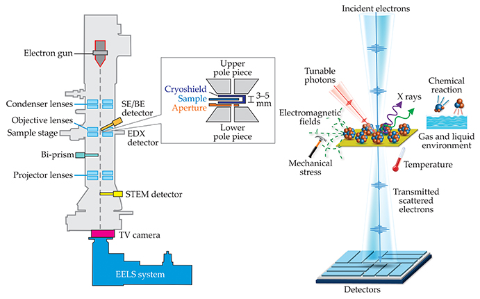
An objective lens typically consists of upper and lower pole pieces. The sample sits in the pole-piece gap. A strongly focusing lens requires a small pole-piece gap, usually ranging from 3 mm to 5 mm (see inset of figure 1), which limits a sample’s maneuverability and environmental conditions. A scanning transmission electron microscope (STEM) is a type of TEM that scans a focused electron beam across the sample in a raster.
Electron–sample interactions generate various signals that often can be acquired simultaneously. The signals can be used for imaging and diffraction and, via energy-dispersive x-ray spectroscopy (EDX) and electron energy-loss spectroscopy (EELS), for chemical analysis. In EDX, an incident electron ejects a core-shell electron from a sample and creates an electron hole. An electron from an outer shell then fills in, and the energy difference between the two shells is released in the form of an x ray that can be used for elemental and chemical analysis. In EELS, the core electron is excited to an unoccupied state; the probe electron loses a corresponding amount of energy during the process. Analysis of the electron energy-loss spectrum’s fine structure provides information not only on the local density of unoccupied states but also on angular momentum and the sample’s chemical nature.
Seeing smaller
Since the invention of the electron microscope, researchers and engineers have continued to improve its spatial resolution. Progress in the late 20th century was staggering. Resolution improvements down to 1–2 Å were largely due to better lens designs, improved electron sources, increased mechanical and electrical stability, and the use of high accelerating voltages. The real breakthrough, however, was the development of aberration correctors for the image-forming lenses in TEMs and the probe-forming lenses in STEMs. Both spherical (wide-angle) and chromatic (energy-dependent) aberrations cause an electron beam to deviate from the ideal paraxial optics and therefore blur the image.
As Otto Scherzer discovered more than 50 years ago, spherical and chromatic aberrations are unavoidable for round lenses. An aberration corrector uses multipole lenses without rotationally symmetric electromagnetic fields. Precise alignment of the corrector elements, which is essential, only became possible with modern computer and feedback technology. Today aberration-corrected TEMs and STEMs can generate images with 50-pm resolution. The probe corrector is typically located above the sample, and the imaging corrector is below the sample.
The two microscopes are complementary. TEM offers high acquisition speed, and STEM is ideal for imaging with atomic-number (Z) contrast. Aberration correction in TEM increases its resolution—in particular its image contrast—but caution is needed for image interpretation. In STEM, the corrector makes possible a larger numerical aperture of the lens, which enables a subangstrom probe with very high current for atomic imaging and spectroscopy.
Aberration correctors significantly enhanced our capabilities in electron-beam nanoscale characterization. Hundreds of aberration-corrected TEM and STEM systems are now operating at 60–300 keV worldwide. Subangstrom-resolution imaging and spectroscopy is not only used in large institutions. Today university researchers can examine in detail the cross section of a heterogeneous two-dimensional interface. Using atomically resolved spectroscopy, they can visualize not only interfacial atom arrangements—including cation displacements associated with local electric polarization, and individual impurity atoms and dopants—but also interfacial electronic states and charge-transfer.
Despite the past success of electron microscopy, further improvement in spatial resolution is no longer compelling on its own. Scientists are strongly motivated to determine the functionality of materials at atomic or molecular resolution, at short time scales, and in real environments. Materials have complex 3D arrangements of atoms and defects that directly determine their utility for applications. Consequently, future opportunities are in 3D imaging of defects, dopants, impurities, and vacancies, along with chemical identification of those impurities in the energy domain to correlate their behavior with different states of electrons.
Modern electron microscopes allow researchers to image individual atoms and acquire single-atom spectra of solids in vacuum. But scientists increasingly need time-resolved, atomic-level imaging and spectroscopy in liquids and gases, during electrochemical deposition, and for oxidation and corrosion reactions as they happen, all under various applied stimuli (see the right panel in figure 1). To control materials properties and behavior will also require pump–probe-based ultrafast techniques that access the natural length and time scales of the involved elementary processes. Let’s now look a bit closer at what might lie ahead.
Seeing in multidimensions
In his 1959 talk “There’s Plenty of Room at the Bottom,” Richard Feynman asked, “Is there no way to make the electron microscope more powerful?” That question had a significant impact on the development of aberration-corrected electron microscopes and on worldwide nanoscience initiatives. However, a challenge beyond Feynman’s vision of understanding the quantum world of materials is to develop atomic-resolution multidimensional microscopes to locate and identify all atomic species in complex systems. The term “multidimensional” refers to the combination of real space, momentum space, energy, time, and additional external parameters like temperature and mechanical stress (see figures 1 and 2).

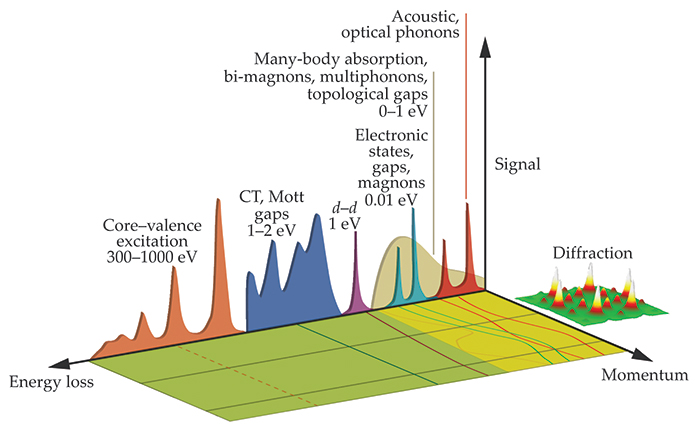
Figure 2. Exploring momentum space and energy space with electrons. The various spectra illustrate the taxonomy of excitations as they become accessible to electron energy-loss spectroscopy (EELS) in electron microscopes. With increasing energy resolution, phonons and electronic excitations in the valence shell will become visible. Mapping of different excitations in momentum space is indicated by the diffraction pattern to the right. Whereas core–valence excitations show no change with momentum, many excitations at low energy do display such energy–momentum dispersions. At intermediate energies, electronic excitations within the d shell of transition metal ions (d–d), charge-transfer excitations (CT), and excitations across the gap of Mott insulators display reduced dispersions. (Courtesy of Fabrizio Carbone and Brookhaven National Laboratory.)
The properties of materials are determined by collective and coupled interactions that are at the heart of some of the deepest unsolved mysteries in condensed-matter physics. Intriguing properties often result from nanoscale electronic inhomogeneity, broken symmetry, or phase separation. Understanding, controlling, and manipulating those local phenomena require imaging not only the real-space atomic structure but also the electronic and spin structures—that is, multidimensional imaging.
The rapid development of electron tomography, which benefited from aberration-corrected electron optics, led to the 3D visualization and analysis of materials’ structures and chemistry at the nanoscale. When tomography is combined with off-axis electron holography and novel reconstruction algorithms, scientists can even map electrostatic and magnetic potentials in practical devices, such as p–n junctions.
One main challenge for future 3D imaging is to resolve and identify individual impurity atoms in materials, including in amorphous compounds with different chemical species. In addition, radiation damage will become an increasingly important issue because tomography entails acquiring a series of images, which will subject the samples to significantly higher electron doses. Low-energy electrons under low-dose operation may prove useful in future instrumentation.
Because EELS offers the possibility of probing the energy and momentum dependence of fundamental excitations, it exceeds the capability of EDX, which is mainly used for composition analysis. When a sufficiently small probe excites electrons only on a single atom or atomic column, site-specific information on the core-level binding energy can be obtained. Analysis of EELS data—particularly at low temperatures where many interesting phenomena occur in condensed matter—gives information on electronic states, including on spin and orbital angular momenta.
The low-energy-loss regime provides information on many collective excitations, as shown in figure 2. Currently, most of the low-energy excitations are not accessible to EELS due to limited energy resolution, typically 0.5–1 eV. If, however, researchers can achieve an energy resolution 2 of a few meV, then both optical and acoustic phonons, magnons, and many-body absorptions can be observed. Such a new capability will allow scientists to directly examine how the structures of interfaces, defects, inclusions, impurities, and local bonding correlate to the subtle changes of the phonon spectra. In turn, that knowledge is relevant to a wide range of frontiers, such as phonon scattering, heat transport, and electron correlation.
Another benefit of the electron probe is that it views a much larger volume in momentum space than x rays do because of the electron’s short wavelength. A new direction for EELS will be angle- resolved measurements, similar to angle-resolved photoemission spectroscopy, but on individual atoms in a bulk material. For that capability to become routine, major instrumentation developments are required, including new ultra-bright electron sources, significantly improved electronic and mechanical stability, revolutionary electron optics designs, and operation at liquid-helium temperatures. Energy–momentum space, represented by the base plane in figure 2, might then become accessible to electron microscopes.
Seeing materials in action
The design of new devices strongly depends on discovering novel materials and understanding those materials’ behavior under external stimuli, as illustrated in the right panel of figure 1. As the size of bit elements in nonvolatile memory-storage devices has shrunk ever smaller, researchers have increasingly turned to electron microscopy to characterize ferromagnetic and ferroelectric nanostructures and their switching behavior in situ. Domain-engineering and strain control of switchable, spontaneous polarization were also recently targeted for ferroelectric FETs.
Currently, magnetic TEM, called Lorentz microscopy, with variable applied magnetic fields is widely used to reveal previously unknown spin configurations. In addition, techniques using continuous electron beams in a conventional TEM to measure gigahertz resonances and pulsed excitations in situ have been developed to study spin-torque effects. A piezo-driven needle built into a sample holder is used to apply a local electric or magnetic field on a nanometer-sized area in the microscope to study the magnetoelectric behavior of a memory device. The same technique can track ionic transport in lithium-ion nanobatteries.
Experiments with bulky sample environments that mimic samples’ working conditions mainly use x-ray and neutron scattering. But those methods often only provide averaged structure information. Proximal-probe approaches, including atomic force microscopy and scanning tunneling spectroscopy, offer information on the local electronic structure and have revealed electronic inhomogeneity and phase separation, but they are surface sensitive, and external stimuli are difficult to apply.
Electron microscopy is the method of choice to reveal local atomic, electronic, and spin structures, which are critical to understanding materials’ behavior at the nanoscale. 3 It is the only method that allows scientists to perform atomic imaging, diffraction, and spectroscopy on the same spot in a weakly scattering object—for example, a single-wall carbon nanotube or graphene.
Aberration-correction technology makes it possible to widen the gap between the pole pieces (see the inset of figure 1) of the objective lens without compromising much spatial resolution. A 1-cm or larger pole-piece gap would provide much needed space for more sophisticated sample holders for in situ imaging and measurements under applied stimuli.
Another longstanding challenge in in situ electron microscopy is to image and determine the electronic states of atoms, ions, and vacancies in gas and liquid environments. Imaging, even at low magnifications, can pose major problems in the presence of the gas or liquid. High-energy electron beams are ideal for penetrating thick cells that allow liquid to circulate or inject gas at pressures close to that of the atmosphere. However, they induce more knock-on damage to the samples. Low-energy electrons, on the other hand, interact more strongly with matter than high-energy electrons, so they generate better image contrast. But they also interact more strongly with the cell membranes, which results in lower signal and higher background.
Radiolysis, in which molecules in a sample chemically dissociate, is another radiation damage mechanism that can be a major issue with liquids and gases, but it usually does not depend on the electron energy. An alternative is to use open-cell configurations. Those configurations work for low-vapor-pressure ionic liquids; for gases they use differential pumping systems with up to 20-torr gas pressure in the microscopes.
To detangle a sample’s structural dynamics and chemical reactions from artifacts due to a gas or liquid environment, researchers have to understand the complex electron-beam-induced effects. Low-electron-dose imaging and fast data acquisition, approaches similar to those used in structural biology, are essential to minimize unwanted artifacts.
Seeing ultrafast
The ongoing development of ultrafast imaging and diffraction opened a new frontier for studying structural dynamics at the nanoscale. Ultrafast electron microscopy combines the superior spatial resolution of conventional electron microscopy with femtosecond electron pulses to detect electronic and atomic motions at their natural time and length scales. 4 Whereas electrons in solids typically travel with the Fermi velocity (usually several nanometers per femtosecond), lattice vibrations propagate with the speed of sound (usually several nanometers per picosecond). Those simple estimates illustrate the temporal resolution required to probe such motions and the intrinsic coupling mechanisms between them.
The nanometer-focused beam in a present-day ultrafast electron microscope can contain just one or a few electrons per pulse. 4 Using one-electron pulses circumvents a significant limitation for multielectron pulses: beam deterioration and image blurring due to the repulsive electron–electron Coulomb interaction. However, a decent image requires a multimillion-shot accumulation of data. The technique is only feasible with instruments that operate at megahertz repetition rates, and it only probes repeatable events. In addition, the sample must return to its initial state before the next electron pulse arrives.
Irreversible phenomena require that images be taken by individual electron pulses containing about 106 or more electrons. Single-shot ultrafast electron microscopes, such as the one developed at Lawrence Livermore National Laboratory, have to operate with about 1-µs pulses for nanoscale imaging to preserve electron beam quality. Future instruments that pack more electrons into each ultrashort pulse while preserving the beam quality will require higher electron-beam energies than current instruments.
Among state-of-the-art electron sources, only photocathode RF guns developed for x-ray free-electron lasers (XFELs), such as the Linac Coherent Light Source at SLAC, are capable of generating more than 107 multi-MeV electrons per subpicosecond pulse. The distinct merit of photocathode RF guns is the very high acceleration gradient (greater than 100 MV/m)—more than two orders of magnitude higher than typical DC guns. It minimizes the electron–electron repulsion effect, which scales as 1/(v2E3), where v is the velocity and E is the energy of the electrons. Photocathode RF guns yield much higher current density and significantly improve beam brightness, as recently demonstrated at Brookhaven National Laboratory.
An additional important advantage of MeV electron beams is that the relativistic speed of their electrons essentially eliminates the velocity mismatch between electromagnetic pump pulses and the probe electrons. The MeV electron beams also penetrate thicker samples and produce easier-to- interpret data because they reduce multiple scattering. Significant challenges lie ahead in the development of ultrafast electron microscopes, whether they are modifications of commercial TEMs or custom-built accelerator-based instruments. However, those challenges are outweighed by the scientific opportunities such instruments would unlock. Here we use the complementarity of electrons and XFEL-based x rays as a guide to illustrate some of those opportunities.
Seeing in time
Energy transport at the nanoscale is crucially important for a wide range of materials. 1 One example that we encounter on a daily basis is heat management for modern microprocessor chips in computers, for which overheating is a significant performance limit. The ability to tailor heat dissipation in new materials and nanostructures is handicapped by how well scientists can detect and understand energy transport as it occurs at microscopic length scales and across interfaces. The experimental challenge is to pinpoint the scattering events that lead to changes in local phonon populations during heat transport.
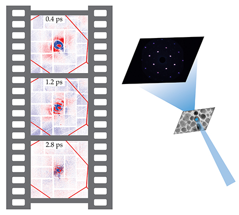
Rather than operate in the frequency domain, where quasiparticle excitations such as phonons appear as discrete energy-loss features in spectra (see figure 2), time-resolved techniques detect the coherent oscillations of phonons in momentum space as they evolve in time. The left panel of figure 3 shows a recent example from a femtosecond x-ray pump–probe experiment. 5 Collective atomic oscillations (phonon modes) lead to diffuse scattering intensity away from Bragg diffraction peaks. The distance from a Bragg peak to the position of such diffuse scattering in momentum space gives the wavevector of the propagating phonon. The phonon frequency is obtained via the Fourier transform of the time-resolved diffuse scattering signal’s coherent oscillations.

Figure 3. Time-resolved diffraction offers a radically new way to observe quasiparticle motion in solids. Femtosecond x-ray diffraction snapshots (left), taken stroboscopically after exciting a germanium single crystal with a 100-fs optical laser pulse, display oscillations in the diffraction intensity due to phonon excitations. The temporal Fourier transform of the combined diffraction patterns results in the phonon excitation energy at each detector pixel, which corresponds to a position in momentum space. Red lines bound the germanium Brillouin zone, the primitive cell in the reciprocal lattice of the crystal. (Adapted from ref.
Time-domain measurements retain information about the phase of the quasiparticle motion. They provide a powerful way to study in microscopic detail the coupling between quasiparticle modes in emergent order and to probe excitations in materials far from equilibrium. Such measurements have only now become possible with XFELs, 5 and the first demonstration experiments are being performed at existing ultrafast MeV electron diffraction sources. However, neither technique has achieved the needed resolution in real space.
Ultrafast MeV electrons offer scattering cross sections many orders of magnitude higher than those of x rays at comparable wavevectors. That advantage is especially important given the inherently low intensity of diffuse scattering signals. However, ultrafast electron microscopy’s greatest virtue is that it is the only technique that can simultaneously achieve femtosecond time and nanometer spatial resolutions. The right panel of figure 3 illustrates a possible future implementation in which a tightly focused electron beam detects a local time-resolved diffraction pattern with nanometer-scale spatial resolution. With such an instrument, researchers could, for instance, directly visualize nanoscale heat transport and study phonon scattering mechanisms as they evolve in time and space after localized energy deposition.
Detection of coherent quasiparticle excitations is central to the study of strongly correlated electron systems. The competition between various degrees of freedom, be they spin, orbital, charge, or lattice, makes those systems sensitive to external perturbations. That sensitivity can be used to control their spectacular materials properties; high-temperature superconductivity is probably the best-known example. The relevant energy scale for quantum emergence, determined by the energy differences between competing ground states, is thought to be in the terahertz frequency range (1 THz corresponds to about 4 meV).
An interesting prospect is to control materials’ properties via terahertz excitations. In recent experiments, researchers triggered the emergence of transient superconducting behavior in the charge- and spin-ordered insulating state of a cuprate compound by exciting a resonant terahertz lattice vibration. 6 The findings are provocative, and the search for competing phases is a hot topic. However, the ground states of high-temperature superconductors, and quantum materials in general, are well known to be spatially inhomogeneous at the nanoscale. If ultrafast electron microscopy is able to measure at the length scale of crystal imperfections a sample’s response to tailored photonic excitation, it would transform the field. Ultrafast electron microscopy would also give unambiguous access to lattice excitations coupled to the spin and charge degrees of freedom in many other quantum materials.
Another recent experiment used multicycle terahertz optical pulses to produce coherent, coupled electronic and magnetic excitations, called electromagnons, in a multiferroic material. 7 Such studies explore quasiparticle interactions and phase transformations induced by strong electric fields. Strong pulses should switch the electric polarization state and, in turn, may influence magnetic order in those materials (see figure 4). 8

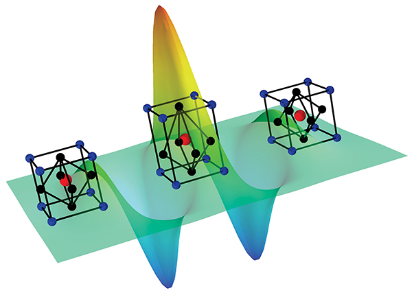
Figure 4. A schematic time–electric field representation of an electromagnetic pulse generated by a femtosecond laser or electron accelerator source. Pulses in the terahertz frequency range can directly couple to the ferroelectric polarization in so-called multiferroic materials, which are characterized by strong coupling between electric, magnetic, and lattice polarizability, indicated here by the crystal-lattice distortions (not to scale). The availability of such pump pulses will open new opportunities to understand and control materials properties for use in next-generation devices.
Ferroelectric and ferromagnetic heterostructures are expected to enable switching of the ferromagnetic state without applied magnetic fields, and they offer novel ways to magnetically store information. (See the article by Nicola Spaldin, Sang-Wook Cheong, and Ramamoorthy Ramesh, Physics Today, October 2010, page 38 .) Static and even dynamic phase separation scenarios are believed to be common in those materials. Ultrafast electron microscopy will thus enable radically new investigations of the application potential for data storage devices.
Investigations of irreversible processes are also an area for which ultrafast electron microscopy offers a game-changing opportunity. Packing many relativistic MeV electrons into picosecond or even subpicosecond electron bunches will enable stroboscopic snapshot imaging at length scales ranging from nanometers to micrometers. Such a capability would be a boon to many areas, from the study of protein dynamics to advanced materials synthesis and matter far from equilibrium.
Seeing ahead
We have discussed the breakthrough science opportunities and the instrument development needed for future electron microscopy. Clearly, electron microscopy will experience revolutionary growth in capabilities in the next decade, from ultrasmall to ultrafast and to multidimensions. Probing materials’ functionalities in situ and in operando with high spatial and temporal resolution will continue to be a main theme. Although instrumentation is often specific to individual fields, there are cross-cutting areas for instrument development, including brighter electron sources, faster detectors, and dedicated spectrometers. As modern science moves from studies of structure and ground states to dynamics and functionalities, such developments could result in transformative advances in many fields of science and engineering.
References
1. US Department of Energy, Office of Basic Energy Sciences, Future of Electron Scattering & Diffraction: Report of the Basic Energy Sciences Workshop (2014).
2. O. L. Krivanek et al., Nature 514, 209 (2014). https://doi.org/10.1038/nature13870
3. Special issue, “Frontiers of in situ Electron Microscopy,” MRS Bull. 40 (2015).
4. A. Zewail, Science 328, 187 (2010). https://doi.org/10.1126/science.1166135
5. M. Trigo et al., Nat. Phys. 9, 790 (2013). https://doi.org/10.1038/nphys2788
6. D. Fausti et al., Science 331, 189 (2011). https://doi.org/10.1126/science.1197294
7. T. Kubacka et al., Science 343, 1333 (2014). https://doi.org/10.1126/science.1242862
8. D. Daranciang et al., Appl. Phys. Lett. 99, 141117 (2011). https://doi.org/10.1063/1.3646399
More about the authors
Yimei Zhu is a senior physicist in the department of condensed-matter physics at Brookhaven National Laboratory in Upton, New York, and an adjunct professor at Columbia University in New York City and at Stony Brook University in Stony Brook, New York. Hermann Dürr is a senior staff scientist at the Stanford Institute for Materials and Energy Sciences at SLAC in Menlo Park, California, and an adjunct professor at the University of Amsterdam in Amsterdam, the Netherlands.


