The discovery of Ovshinsky switching and phase-change memory
DOI: 10.1063/PT.3.3948


On 11 November 1968 a surprising announcement sent shock waves through the field of solid-state physics. That month Physical Review Letters published Stanford Ovshinsky’s “Reversible electrical switching phenomena in disordered structures.” 1 The paper described an extremely fast threshold switch and an electronic memory made of amorphous materials, feats that had not been thought possible.
In the 1960s crystals were considered the proper subject of the field, and standard textbooks such as Frederick Seitz’s The Modern Theory of Solids typically began with a presentation of the different crystalline structures. That bias was not an irrational prejudice. It followed from the history of the field, which began with crystallography and started becoming systematic in the 1930s with the application of quantum theory. The regular lattice structure of crystals enabled Felix Bloch to simplify his calculations and “explain how the electrons could sneak by all the ions in a metal.” (See his article in Physics Today, December 1976, page 23 .) In time, such work led to the modern theory of solids. 2 Furthermore, crystals had become the basis for the growing semiconductor industry that took off after the invention of the transistor late in 1947; it was supposed that the success of such devices depended on the periodic structure of their crystalline material. There were thus strong theoretical and practical reasons for preferring crystals, and Ovshinsky’s discovery met with predictable resistance.
Some leading scientists, however, were quick to recognize the importance of Ovshinsky’s work. “It is the newest, the biggest, the most exciting discovery in solid-state physics at the moment,” said Nevill Mott, director of the University of Cambridge’s Cavendish Laboratory. Furthermore, Mott noted, unlike the transistor, whose principles could have been worked out from existing knowledge, Ovshinsky’s discovery was “quite unexpected” and “represented totally new knowledge.”
Mott’s praise, quoted in a front-page New York Times article 3 that appeared the same day as the Physical Review Letters paper, gave wider publicity to Ovshinsky’s discovery but also increased the angry response provoked by his challenge to established scientific doctrines. Announcing a scientific finding in a newspaper was seen as unprofessional behavior; its coming from an unknown, unaccredited researcher compounded the offense. As an outsider, a self-educated inventor with no credentials beyond a high school degree, Ovshinsky was regarded by many established researchers as a self-promoting charlatan, and some tried to get the journal paper and newspaper article changed or withdrawn.
To the further outrage of leading industrial researchers, the Times account even suggested that this new “glassy electronic device” might replace the transistor, already the basis of a billion-dollar electronics industry. That has not happened, but the discovery of the Ovshinsky effect, the fast and reversible switching between resistive and conducting states in amorphous semiconductors, has led to growing research in materials science and to important new information technologies.
How did this outsider, working alone in a Detroit storefront, make a discovery that helped change the basic paradigm that solid-state physics was primarily a study of crystals? Historical studies of scientific discoveries often show how they depend on a cluster of converging factors. In this case the factors derived from the unusually diverse experiences of Ovshinsky’s career.
Becoming an inventor
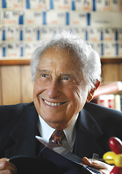
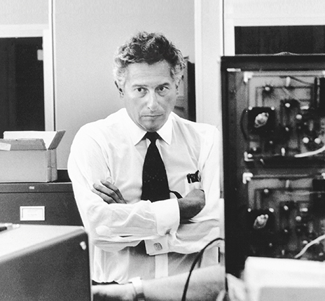
Ovshinsky (shown in later life in figure
Figure 1.

Stanford Robert Ovshinsky in August 2005. (Photograph by Glenn Triest.)
After graduating from high school in 1941, Ovshinsky had no interest in further formal education and devoted himself to becoming a machinist and toolmaker. His earliest inventions grew out of his work in the tool rooms of companies like B. F. Goodrich and Goodyear Aircraft. From the beginning, he thought about ways to improve the design of his tools. By the end of World War II, he had conceived his first invention, an innovative lathe he named the Benjamin Center Drive to commemorate his recently deceased father. As with his later inventions, Ovshinsky did not make piecemeal improvements to an existing design. Rather, he worked from general principles. He understood that vibration and the resulting friction and heat were what limited machining, and he set out to eliminate them by using a heavy, welded-steel base, a massive hydraulically controlled chuck, and an absolute minimum of moving parts.
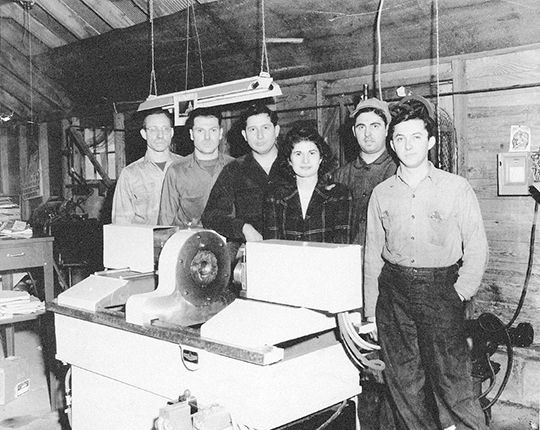
Ovshinsky set up his first company, Stanford Roberts Machine Company, in a barn on the outskirts of Akron. There, in 1946, he built the prototype of his new machine, shown in figure
Figure 2.

The Benjamin Center Drive lathe was developed in a barn in Akron, Ohio. Stanford Ovshinsky (third from left) and his staff pose in this circa-1946 photo. (Courtesy of the Ovshinsky family and the Bentley Historical Library, University of Michigan.)
In addition to the Benjamin lathe, the Ovshinsky brothers worked on automating other machines, including a programmable self-guided tractor. Those projects were never completed, but they contributed to Stan’s development as an inventor by leading him to the new field of cybernetics, whose general principles conflated animate and inanimate intelligence. (The subtitle of Norbert Wiener’s influential 1948 book Cybernetics is Control and Communication in the Animal and the Machine.) That conflation would be crucial for his later work on switching.
At the end of 1951, Ovshinsky moved to Detroit, Michigan, to accept a position as director of research at the Hupp Motorcar Company. He invented several automotive components that use feedback and other cybernetic processes; they include electrical power steering and an electrical automatic transmission. Pursuing his interest in communication and control, he also read extensively in the field of neurophysiology. Soon he was writing papers on neurophysiology, about half a dozen in the early to mid 1950s, some of which were later published. On the basis of one that was not published, “Nerve impulse,” Wayne University Medical School invited him to participate in experimental research on the cerebellums of cats and monkeys, work that led to his later electronic inventions.
Ovshinsky’s nerve-cell analogy
Like other inventors, Ovshinsky often relied on analogy. His papers in neurophysiology repeatedly make analogies between animate motor control and servomechanisms or between neurons and switches. He conceived the nerve cell as a kind of threshold switch that fires when accumulating impulses reach a triggering point; as an inventor, his way of testing that hypothesis was to build a physical model. Working with Herb, he used thin oxide films formed on two tantalum electrodes to model the nerve cell’s semipermeable membrane, which he believed was the locus of the cell’s electrochemical activity. The electrodes were immersed in a liquid potassium hydroxide electrolyte, the analogue of the fluid surrounding neurons.
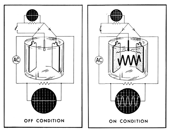
The tantalum oxide insulated the electrodes and prevented the flow of AC current. However, introducing or removing a small DC bias through a third, nonreacting electrode made the device switch on or off (see figure
Figure 3.

The Ovitron, inspired by Stanford Ovshinsky’s conception of the nerve cell, was a fast switch invented by Stan and his brother, Herb, in about 1959. As this promotional diagram illustrates, the device has three electrodes immersed in an electrolyte. The two larger tantalum electrodes are coated with an insulating oxide layer; the third electrode, matchstick-shaped in the sketch, is nonreacting. In the off condition, the smaller electrode is disconnected and AC current does not flow through the two main electrodes. But in the on condition, a DC source establishes a potential difference between the smaller electrode and the other two, which allows AC current to flow through the main circuit. (Courtesy of the Ovshinsky family and the Bentley Historical Library, University of Michigan.)
Those features attracted considerable attention in trade publications such as Electronics and Control Engineering, whose articles about the Ovitron repeated Ovshinsky’s explanations based on his nerve-cell analogy. Subsequent research, however, has clearly shown that the analogy was faulty. The switching is actually the result of deplating and replating the electrodes: The DC bias causes the insulating oxide layer to become thin enough to allow quantum electron tunneling, and removing or reversing the bias induces the oxide to re-form. But as in many other scientific discoveries, faulty assumptions led to an important result.
What was Ovshinsky doing when he created the Ovitron? Was he testing his theory of the nerve cell or trying to invent a new kind of switch? Was he doing science or technology? The answer seems to be “all of the above.” When he began in his later years to reflect more on creativity and how he invented, a recurrent theme was his disregard for divisions between disciplines and his refusal to distinguish between science and technology. A traditionally educated neuroscientist or electrical engineer would not have been likely to arrive at the Ovitron.
The commercial development of the Ovitron was thwarted by legal conflicts with a partner who had provided financing and then tried to take control of the company. Settlement of the ensuing lawsuit in March 1960 provided substantial financial compensation for Ovshinsky, but it also enjoined him from working further on the Ovitron or on any device that used the same design or materials. As it turned out, those restrictions forced Ovshinsky to find different materials and another design and led him to his greatest achievements as an independent inventor.
The search for new materials
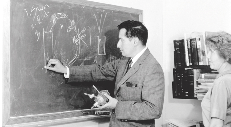
By the time the Ovitron lawsuit had been settled, Ovshinsky was working in a modest Detroit storefront with his partner and later wife, Iris Dibner. Shown together in figure
Figure 4.

Stanford Ovshinsky and Iris Dibner founded Energy Conversion Laboratory to address energy-related social ills. Here Ovshinsky explains one of his alternative-energy plans. (Courtesy of the Ovshinsky family and the Bentley Historical Library, University of Michigan.)
Several strands of Ovshinsky’s experience converged in that event. One of them dates from his years as a machinist, during which he had encountered problems with the limit switches used to stop or turn around the pieces being machined on lathes and milling machines. In an environment of metal chips and cutting oil, those electromechanical switches often failed to turn on when the dirty contacts of the relay touched. Ovshinsky initially saw that failure as an annoyance, but he found that the contacts would conduct when he increased the voltage. As physicist Hellmut Fritzsche related to one of us (Hoddeson) in a 2006 interview, Ovshinsky realized that “if that is so, I don’t need the relay. If that part [the film of dirt] is nonconducting but with the higher voltage it does conduct, it is by itself a switch.”
Another crucial strand came out of his work on the Ovitron, whose switching relied on a thin oxide film on the tantalum electrodes. At some point, Ovshinsky realized that the oxide layer had an amorphous structure. Perhaps he could use a different amorphous material instead of the oxide that he was legally barred from using. Following that hunch, he tried to create amorphous films that, like the insulating film of dirt on the lathe relays, would act as switches. Working through the periodic table of elements, he focused on the chalcogens, the elements grouped under oxygen. Like oxygen, those elements—sulfur, selenium, tellurium, and polonium—have six electrons in their outer shell and a valence of two.
Ovshinsky tried to learn about chalcogenide glasses, and about glasses more generally, but he found little help. He might have found guidance in the work of Boris Kolomiets, who had been studying amorphous chalcogenides in Leningrad since the mid 1950s. But Ovshinsky does not appear to have known about Kolomiets’s work until the mid 1960s. In any case, although Kolomiets reported the semiconducting properties of chalcogenides, he did not observe the switching effect that Ovshinsky would discover, because his experiments used bulk materials instead of thin films.
What does seem to have helped Ovshinsky find the right materials for his new switch was making analogies. He later explained in conversations with Hoddeson that he was especially intrigued by selenium and tellurium because the molecular chain structure of their amorphous forms reminded him of DNA, whose double-helix structure had been described in 1953. The fruitful analogy comparing the structures of amorphous selenium and tellurium with that of DNA bridged organic and inorganic structures, as did the nerve-cell analogy that had motivated the invention of the Ovitron.
Ovshinsky was already prepared to appreciate the significance of chain structures because of another strand of experiences that dated back to well before his work on switches. While at B. F. Goodrich in 1941, he had taken a seminar on the chemistry of rubber; in it he learned that rubber is a polymer composed of long molecular chains connected by cross-links. The analogy between the structures of rubber and DNA engaged Ovshinsky’s distinctive ability to visualize molecules. In a 2011 interview with Hoddeson, he described his search for new switching materials: “I wanted something that could have cross-links, and none of the elements except the chalcogens really has that. I wanted something that has built-in plasticity and flexibility,” presumably because he believed that would facilitate making thin films. “And because I was brought up in Akron, Ohio, I was familiar with polymers and cross-links. Because that’s what rubber tires are made out of.” Ovshinsky’s choice of the chalcogens, and ultimately of tellurium, was thus mainly intuitive, based on several hunches and analogies deriving partly from recent work and partly from his past experience. The role of the cross-links was explained in microscopic terms only later, when he could collaborate with trained physicists to publish scientific accounts of his discoveries.
The Ovshinsky effect
Ovshinsky soon found that to get the switching he wanted, he had to combine tellurium with elements like arsenic and antimony from neighboring groups of the periodic table. He could not afford expensive evaporation and deposition equipment for creating thin films, so he ground his materials into powders, combining and pressing them into thin layers. That technique, too, drew on earlier experience. In the early 1940s, Ovshinsky had done related metallurgical work when he had hot-pressed powders and attempted to get as many different elements as possible to hold together. In 1961, to try different combinations and proportions of elements, he built a small box he called his universal tester, in which he pressed together various powders and probed them with the leads of his homemade Heathkit oscilloscope. He sometimes saw an erratic switching effect, but he did not yet have a reliable switch.
Then a new possibility occurred to him. The powders in the stagnant air of the ECL storefront had given Ovshinsky a mild case of arsenic and tellurium poisoning, but they also gave him an idea. Suspecting that the polluted air had deposited an invisibly thin film on the micrometer he would carry in his toolmaker’s apron for measuring thicknesses, he attached an AC power source across the calipers and connected the leads to his oscilloscope. Closing the calipers, he gradually increased the voltage and observed the current flowing across the film. Suddenly, a persistent and dramatic cross pattern appeared on the screen, such as the one shown in figure
Figure 5.

An oscilloscope cross pattern demonstrated that Stanford Ovshinsky had created an amorphous threshold switch. The path of a bright spot on the screen indicates voltage on the horizontal axis and current on the vertical axis. As the voltage applied to the switch alternates 60 times per second, the spot moves so rapidly that the eye sees the spot’s path as a trace. Amorphous materials normally have so high a resistance that the current remains very small. But for Ovshinsky’s film, when the voltage reaches a positive or negative threshold value, the material becomes so highly conducting that the oscilloscope spot jumps up or down almost vertically. Sweeping the voltage further returns the trace to zero and completes the cross. (Courtesy of the Ovshinsky family and the Bentley Historical Library, University of Michigan.)
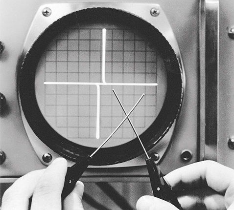
That was the eureka moment. The oscilloscope cross indicated an extremely rapid, almost instantaneous switching from resisting to conducting and back each time the amplitude of the voltage crossed a threshold. The symmetry of the cross showed that the behavior of the switch, unlike that of a diode or transistor, was reversible. No one else had seen the effect before. Ovshinsky’s hunch about making switches from thin films of amorphous materials had been spectacularly confirmed.
He immediately sensed the importance of his discovery and worked to reproduce the switching effect reliably. By October 1963 he had not only submitted a patent application for the threshold switch
4
but was also publishing data on his chalcogenide switches based on tellurium alloyed with arsenic, silicon, and germanium. Magazine articles in Electronics and Control Engineering featured the Quantrol, Ovshinsky’s name for the new device before he renamed it the Ovonic Threshold Switch. The piece in the April 1964 issue of Control Engineering seems to be the first that received much attention.
5
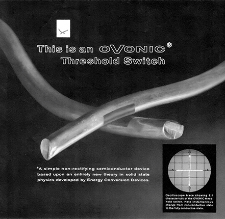
Ads from the time featured an elegant image, shown in figure
Figure 6.

This Ovonic switch advertisement from the mid 1960s touts “an entirely new theory in solid state physics.” The iconic oscilloscope cross pattern appears at the lower right. (Courtesy of the Ovshinsky family and the Bentley Historical Library, University of Michigan.)
Almost in passing, the last section of the Control Engineering article mentions a memory device whose invention was a serendipitous offshoot of the threshold-switch research, an accident that Ovshinsky’s prepared mind was able to interpret and seize upon. One day, his part-time assistant, who was studying how the switching behavior changed with different proportions of the materials in the amorphous film, came to Ovshinsky very upset. One of the devices he was testing remained in the low-resistance conducting state rather than switching off, so he had thrown it away. Ovshinsky, however, retrieved the discarded device from the trash and gave it a stronger pulse. It again switched and became nonconducting. Right away, he recognized the significance of what he had: a bistable memory device. Based on a slightly different composition of the material used in the threshold switch, it became the basis of a fast rewritable electrical memory. Later known as phase-change memory because it switched between amorphous and crystalline states, it would eventually be acknowledged as one of Ovshinsky’s most significant discoveries.
Commercialization
The path to realizing the full potential of phase-change memory has already proved to be longer than the path leading to its discovery. The recognition of Ovshinsky’s discoveries helped make the study of amorphous and disordered materials a respectable and growing research field. At the same time, commercial interest and government support provided the resources that enabled him to transform ECL into a much larger R&D organization, Energy Conversion Devices (ECD).
With its growing staff of trained researchers and its cohort of accomplished scientific consultants, ECD developed numerous technologies based on amorphous and disordered materials. For example, Ovshinsky invented a machine for mass-producing thin-film amorphous silicon solar panels; eventually ECD’s subsidiary United Solar would become their largest manufacturer. His disordered hydrogen-storage materials became the basis for the nickel–metal hydride battery, which continues to be widely used.
The development of ECD’s more radically innovative information technologies, however, faced greater difficulties. The first commercial success of phase-change memory was its optical version, in which the transition between amorphous and crystalline states is induced by a laser. It became the basis of the rewritable CDs and DVDs that were widely used in the 1980s and 1990s and are still in use today.
But the far more promising electrical version of phase-change memory has taken half a century to come into its own. The challenge has been to compete successfully with flash memory, which for two decades has dominated the market in personal computers, smartphones, and other devices. Chalcogenide-based phase-change memory has many advantages over silicon-based flash memory: It is much faster, requires less power, and is capable of orders of magnitude more rewrite cycles. But it is also more expensive, and what the market wants, as one of Ovshinsky’s scientists commented to us, is “cheap and good enough.” For a long time, flash memory has been cheap and good enough.
When Ovshinsky died in 2012, his Ovonic phase-change memory was still waiting for its time to come. To the physicists and engineers who had worked on it at ECD or its subsidiary Ovonyx, the eventual commercial adoption of phase-change memory seemed inevitable. Sooner or later flash memory would reach its limit for scaling down in size, but chalcogenide phase-change memory works better as it scales down because of its lower power requirements. Most of the ECD veterans thought, however, that decades would pass before that happened. It was therefore a surprise when in a July 2015 press release, 6 Intel Corp and Micron Technology, the companies that had acquired ECD’s and Ovonyx’s relevant patents, announced their 3D XPoint memory, “a major breakthrough in memory process technology and the first new memory category since the introduction of NAND flash in 1989.”
Intel and Micron were at first secretive about the composition and origins of the new device. To Ovonyx veterans, however, it was clear—and was later confirmed—that the design at the heart of 3D XPoint memory was essentially the one they had developed at ECD by 1989, with Ovshinsky’s threshold switch as its access device and his phase-change memory as its storage element. 7 The 3D XPoint chip was commercially released in mid 2017, under the brand names Optane and QuantX. Given its potential to enable significant advances in information technologies, the discovery Ovshinsky made more than 50 years ago in his Detroit storefront will likely play an important role in the information economy of the 21st century.
The outsider and the disciplines
Ovshinsky’s discoveries of amorphous semiconductor switching and phase-change memory owed much to his position as an outsider. Untrained in science and unconstrained by disciplinary orthodoxies and divisions, he pursued analogies and played hunches that led him outside the then current paradigm of solid-state physics. One could view the subsequent validation of his discoveries and the growing importance of amorphous and disordered materials in science and technology as the triumph of a heroic independent outsider over the insiders who tried to dismiss him. But that account would miss the full complexity and interest of his story.

COURTESY OF THE OVSHINSKY FAMILY AND THE BENTLEY HISTORICAL LIBRARY, UNIVERSITY OF MICHIGAN
To appreciate that complexity, it helps to set Ovshinsky’s story in a longer historical perspective. Before the 20th century, it was not uncommon for brilliant self-trained individuals like Michael Faraday to make scientific breakthroughs. But as disciplines became established and maintained by degree-granting academic programs and other institutions such as scientific societies and journals, working outside disciplinary boundaries became much more difficult. It is thus not surprising that when Ovshinsky announced his discovery he encountered suspicion and that when his discovery challenged established doctrines he encountered outright hostility: Such is the typical response of a community to an outsider who violates its norms.
But if Ovshinsky’s breakthrough discovery was the accomplishment of an isolated individual, his later success depended on the collaboration of the many scientists at ECD and Ovonyx who solved the difficult technical problems involved in realizing his ideas. Similarly, in communicating his findings to both specialized and general audiences, he depended on consultants and staff who could describe his work in scientific terms and explain it more clearly than he could. Despite his resemblance to earlier independent scientists, Ovshinsky’s advancement beyond his pivotal discoveries was enabled by the established scientific disciplines and the highly trained researchers they produced.
Supplemental Material
The Henry Ford Museum of American Innovation has posted several interviews with
This article is based on our book The Man Who Saw Tomorrow: The Life and Inventions of Stanford R. Ovshinsky (MIT press, 2018).
References
1. S. R. Ovshinsky, Phys. Rev. Lett. 21, 1450 (1968). https://doi.org/10.1103/PhysRevLett.21.1450
2. See L. Hoddeson, G. Baym, M. Eckert, in Out of the Crystal Maze: Chapters from the History of Solid-State Physics, L. Hoddeson, E. Braun, J. Teichmann, S. Weart, eds., Oxford U. Press (1992), p. 88.
3. W. K. Stevens, New York Times, 11 November 1968, p. 1.
4. S. R. Ovshinsky, “Symmetrical current controlling device,” US Patent 3,271,591 (6 September 1966).
5. M. P. Southworth, Control Eng. 11, 69 (1964).
6. “Intel and Micron Produce Breakthrough Memory Technology,” Intel news release, 28 July 2015 .
7. J. Choe, “Intel 3D XPoint memory die removed from Intel OptaneTM PCM (Phase Change Memory),” Tech Insights (18 May 2017);
R. Merritt, “3D XPoint steps into the light,” EE Times (14 January 2016).
More about the authors
Lillian Hoddeson is a professor of history emerita and Peter Garrett is a professor of English emeritus, both at the University of Illinois at Urbana-Champaign.


