Quantum size effects in metallic nanostructures
DOI: 10.1063/1.2731973
In solid-state physics, crystals are usually assumed to be large enough that the influence of finite dimensions on their electronic structure is negligible compared to the effects of the periodic potential produced by the regular arrangement of the ion cores. The energy of a nearly free valence-band electron in a metal can then simply be described by its dependence on the wave vector k = (2π/λ)e, where e is a unit vector in the direction of propagation of the electron and λ is its wavelength.
When one or more dimensions of the crystal approach interatomic distances or the electron’s wavelength, however, the electron feels the effects of the crystal boundaries in addition to the periodic potential. The potential outside the solid is drastically different from the one inside. The influence of the boundaries is clearest in the context of the jellium model, in which the positive ion cores are smeared out as a homogeneous positive background. Inside the solid, the electron energy E(k) follows a simple parabolic form. The role of the boundaries is to severely restrict the allowed wave vectors that electrons can adopt inside the crystal.
Ultrathin films, two-dimensional islands, and one-dimensional wires can be prepared using epitaxial methods and can exhibit what are known as quantum size effects (QSEs) that arise from the confinement of electrons. Because the electron in any of those structures is reflected at the boundaries, the total phase difference accumulated by the reflections must be a multiple of 2π according to the Sommerfeld–Bohr quantization rule
Here, k z is the allowed wave vector component normal to the surface, n takes on integer values, d is the crystal thickness, and φ1 and φ2 are phase terms that account for wavefunction leakage beyond the potential steps at the film boundaries.
Researchers have known for decades that decreasing the thickness of a metal film alters its electronic structure. 1,2 Indeed, QSEs can appear as dramatic oscillations in properties as varied as the conductivity, surface energy, Hall effect, and chemical reactivity. Remarkably, the reverse is also possible: Varying the energy levels in a film offers a path to precisely control the size and geometry of structures that grow on a surface. Our goal in this article is to bridge the early work on QSEs in metal films with the recent interest in the controlled growth of nanostructures.
QSE phenomena may be divided into two groups: those involving bound states, for which a quantum well is the usual description, and those involving free states, mainly those of electrons above the so-called vacuum level—that is, having kinetic energy greater than zero. In the latter case, the potential in the film determines the transmitted and reflected intensities of an incident electron wave. The optical analog is the Fabry–Perot etalon, in which changes either in the distance d between two reflectors or in the wave vector k z of the incident wave produce oscillations in the intensities of transmitted and reflected waves. Both groups of phenomena—whether explored using quantum-well or Fabry–Perot descriptions—have been investigated since Robert Jaklevic 3 and Richard Thomas 4 first observed them more than 35 years ago.
Before discussing the QSEs, we note a few preliminaries. First, the direction of the wave vector of incident electrons used in Fabry–Perot-type experiments can be controlled and is usually restricted to the z axis, normal to the crystal surface. In contrast, the wave vectors of bound-state electrons within the film can point in all directions of space. Second, the jellium model of a crystal is generally a crude approximation; the real band structure E(k) of the crystal has to be taken into account to accurately determine the quantization condition.5 Third, the thickness of a film cannot be changed continuously but only in discrete monolayer steps, typically 0.2–0.3 nm in height.
Bound states
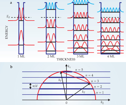
In bulk, nearly free-electron metals, the Fermi surface can be represented as the surface of a sphere whose radius k F is determined by the electron density ρ. The relation k F = (3π 2 ρ)1/3 also defines the Fermi wavelength λ F = 2π/k F. The electrons occupy quasi-continuously distributed states inside the Fermi surface. In a thin film, the quantization of the wave vector k z divides the Fermi sphere into discrete subbands and causes a host of electronic properties to oscillate as the thickness varies over a period of half the Fermi wavelength. 2
To see how those oscillations arise, take an infinitely deep well of width d to approximate a flat film of thickness d. A new QSE level moves below the Fermi level with each λ F/2 increment in d, because the nodes of the electron’s wavefunction remain pinned to the boundary. More realistically, the confining well has finite depth and the wavefunction— or more physically, the charge—leaks out as shown schematically in figure 1a. A dipole forms at the vacuum–film interface with a strength that oscillates with the separation of the highest occupied band from the Fermi level and therefore with d. This oscillating dipole produces accompanying oscillations of the work function, electron density, and surface energy. 1,2,5

Figure 1. (a) This set of finite quantum wells represents the confinement of electrons in ultrathin metallic films whose thicknesses vary from one to four monolayers (ML). The squares of the electron wavefunctions in each quantum level are plotted on top of the corresponding occupied (red) and unoccupied (blue) states; the dashed lines for each film mark the Fermi level E F. As the principal quantum number n increases in each well, so does the fraction of an electron’s wavefunction that leaks out past the boundaries. (b) In a metal, electrons occupy nearly continuously distributed states inside the Fermi surface, often represented as the surface of a sphere of radius k F. In an ultrathin metal film of thickness d, quantization of the wave vector normal to the film’s surface, kz , divides the Fermi sphere into a discrete collection of two-dimensional disks or subbands—pictured here in cross section—each separated by Δkz = π/d for the ideal case of an infinitely deep well. As the film thickness increases from a single monolayer, additional subbands defined by n fall below E F. The effect is a periodic modulation of the electron concentration, scattering rate, and other electronic properties because new quantum states become available. The diagram pictures the scattering of an electron from subband n = 3 into n = 5 in a three-monolayer-thick film.
Figure
QSEs are most clearly observed when n and d are small—that is, when the separation between energy levels is large enough to exceed their broadening due to inelastic scattering or inhomogeneities in the film. In metals, that condition is typically fulfilled when the film is only a few monolayers thick, nearly perfectly flat, and highly crystalline. Modern growth techniques such as molecular beam epitaxy make preparing films with those characteristics routine.
Photoelectron spectroscopy can be used to directly determine the discrete energy levels of QSE states in electron-confining nanostructures. Tai-Chang Chiang and colleagues from the University of Illinois at Urbana-Champaign first demonstrated the technique’s power to measure QSE energies in their 1986 study of silver films grown on a 7 × 7 reconstructed silicon (111) surface. 6 Key to their success was having the films prepared with uniform thickness to within a few monolayers over the area probed by the technique, roughly 1 mm2. That uniformity can be achieved by growing films at low temperature, monolayer by monolayer.
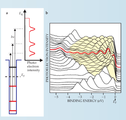
The number of occupied QSE states in metallic films is typically small enough that it is easy to identify the principal quantum number n and therefore the normal component of the wave vector k z from the photoemission spectra. If the parallel component k ‖ can also be deduced, as in angle-resolved photoemission, researchers can reconstruct the in-plane dispersion of electrons E(k ‖) for each subband. Photoelectrons emitted at angle θ with respect to the surface normal carry the parallel wave vector component sinθ, where E K is the electron kinetic energy outside the film. The dispersion of states that form in a 23-monolayer film of aluminum deposited on Si(111) provides a compelling case in point (see figure 2).

Figure 2. Angle-resolved photoelectron spectroscopy measures the kinetic energy E K and momenta of electrons emitted from the surface of a metal film. (a) An idealized spectrum of the kinetic energy of electrons emitted normal to the surface by photons of energy h ν. (b) Photoelectrons emitted at other angles have nonzero parallel components of the wave vector and can reveal details about any state within the Fermi sphere. In this spectrum of a 23-monolayer-thick aluminum film on a silicon (111) surface, each curve corresponds to the photoelectron energy distribution at a particular angle. The features outlined in yellow reveal quantum size effects associated with the direction of momentum of the emitted electrons. The red curve is the spectrum measured for normal emission (k ‖ = 0). The uncolored peaks are Al surface states, unrelated to quantum size effects.
(Adapted from L. Aballe et al.,
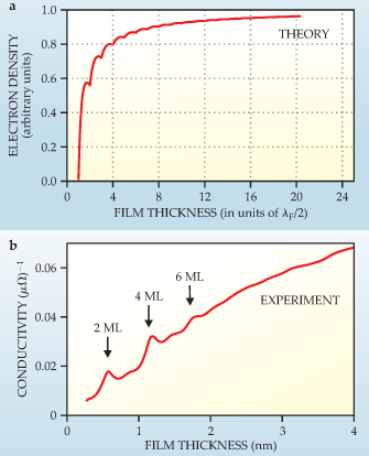
The position and spacing of the discrete energy levels vary with the film thickness. As pictured in figure 1a, whenever a subband crosses the Fermi level, the number of QSE states occupied by electrons increases in a stepwise fashion. The electron concentration and scattering rate thus oscillate with a period of half the Fermi wavelength (see figure 3a). 7 Those two parameters determine the electrical conductivity and other galvanomagnetic properties such as the Hall effect. 8

Figure 3. Electrical conductivity of a metallic ultrathin film. (a) Modeled as an infinite quantum well, the film is predicted to have an electron density that oscillates with a period of half the Fermi wavelength λ F as a function of film thickness. (b) Experimental conductivity of lead deposited on a gold-modified silicon (111) surface, measured in situ during deposition at 95 K. Measuring the conductivity during layer-by-layer growth reveals quantum size effects in the form of peaks at two-monolayer intervals. The peak positions at two, four, and six monolayers (ML) correspond to larger carrier concentrations and smaller scattering rates, which are expected when the highest occupied QSE subband is far from the Fermi level. The weaker modulations at three, five, and seven monolayers come from periodic surface roughness variation that occurs during film growth.
(
The increasing number of QSE states below the Fermi level offers new channels for electron scattering in the vicinity of the Fermi level and reduces the electron mean free path. For instance, figure
Experimentally, the situation can be complicated. The film thickness varies in increments of a single monolayer d 0, and the electrical conductivity can generally be measured only for discrete thicknesses—that is, multiples of d 0. Thin films are commonly made up of areas with different thicknesses. The measured conductivity is then a superposition of different conductivities, which makes observing their QSE oscillations difficult.
Indeed, not until the mid-1980s could ultrathin films be grown with sufficient quality to allow researchers to measure modulations of the electrical conductivity in situ as a function of thickness. But making reliable and stable electrical contacts to the grown film remained difficult.
The first strong experimental confirmation of conductivity on QSEs was presented in a series of publications dating from 1988 on ultrathin films of lead. That year, two of us (Jałochowski and Bauer) managed to grow the films on a gold-modified Si(111) surface at 95 K, a substrate and temperature that assured nearly monolayer-by-monolayer growth.
7
The most pronounced electrical conductivity peaks occurred when the Pb film reached two, four, and six monolayers, as shown in figure
Another QSE of potential practical importance is the stronger bonding of adsorbates and therefore a higher chemical reactivity that accompanies an increased density of electron states at the Fermi level. Three years ago, for example, Lucia Aballe and colleagues found that the oxidation rate of a magnesium film oscillates with the occupation of new quantized states. 9 If QSE films can be grown that are stable under reaction conditions, this effect may become important in heterogeneous catalysis.
Free states
The most direct manifestations of QSEs are the oscillations in intensity of reflected or transmitted electron waves incident on ultrathin films. Unlike the Fabry–Perot etalon, which is symmetric at its boundaries, an ultrathin film is asymmetric: On one side is vacuum; on the other, the solid substrate. In 1970 Thomas first observed such oscillations by transmitting slow electrons through gold films deposited on iridium. 4 Since then researchers have captured the oscillations using grazing-angle reflection of high-energy electrons 10 as well as normal-incidence reflection of slow electrons.
In the slow-electron experiments the intensity oscillations are best seen in atomically flat films using electron energies below 20–30 eV, energies at which electron inelastic mean free paths are large. Details of the oscillation patterns can reveal the film thickness, interlayer spacing, mean potential, and interface properties, in addition to the inelastic mean free path of an electron and the band structure above the vacuum level. In 2003, for example, Michael Altman and coworkers used low-energy diffraction to determine oscillations in the interlayer spacing in a film of silver on tungsten and in the silver–tungsten interface spacing as a function of film thickness. 11
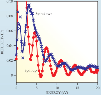
Of particular interest are QSEs in magnetic systems. The exchange interaction splits a subband E(k z , k ‖) into two separate branches, and incident electrons whose spin is parallel to the spins of electrons in a magnetic crystal experience a different scattering potential than electrons whose spins are antiparallel. The different energy dispersions can be deduced from the energy dependence of the reflectivity of spin-polarized electrons, first observed by Danilo Pescia and coworkers in 1991, in copper films on cobalt (100) and in cobalt films on copper (100). 12
Spin-dependent reflectivity oscillations of the kind shown in figure 4 allow researchers to determine the exchange splitting of E(kz ) above the vacuum level in ferromagnetic layers. Spin-dependent reflectivity plays a major role in the giant magnetoresistance effect in ferromagnetic trilayers and superlattices, structures that have widespread use in computer technology. In trilayers a nonmagnetic interlayer serves as the quantum well whose thickness determines the magnetic interaction between the outer ferromagnetic layers. 13

Figure 4. Quantum size effects in magnetic systems. The reflectivity of slow electrons from six-monolayer-thick iron microcrystals on a tungsten surface depends on whether the electrons are spin up (red) or spin down (blue). The exchange interaction accounts for the difference in reflectivity at any particular energy. The reflectivity oscillations of spin-down electrons have smaller amplitudes and larger damping than those of spin-up electrons because spin-down electrons have a shorter inelastic mean free path.
(Adapted from R. Zdyb, E. Bauer,
Tuning the thickness
Our discussion so far has focused on the expectation that as the geometric dimensions of a nanostructure change, so do its electron energy levels. And the degree to which electron energies vary with thickness depends on how far their wavefunctions leak out of the confining well. Seven years ago, researchers realized that variations in energy levels from the confinement of electrons in a thin film could themselves lead to nanostructures that are stable at different thicknesses, or heights.
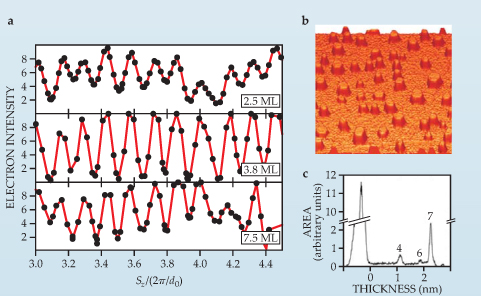
Experiments on the low-temperature growth of Pb on Si reveal the robust formation, induced by QSEs, of Pb islands whose heights reach some uniform, preferred level. One of us (Tringides) and colleagues at Iowa State University used high-resolution low-energy diffraction and scanning tunneling microscopy (STM) to study that growth. The group measured the fringes—that is, variations in the reflected electron intensities—as a function of the normal component of momentum transfer S from incident electrons to the Pb islands. 14 Based on the period of the fringes ΔS z, one can predict the island height d = 2π/ΔSz .
Figure 5 shows that uniformly flat, hexagonally shaped, seven-monolayer islands of various diameters form on 7 × 7 Si(111) at a temperature of 180 K. Although seven monolayers is the most stable Pb-island height, others can be formed, each differing by two monolayers, by carefully controlling the temperature and Pb coverage. 14

Figure 5. Interference of incident electron waves from a thin film indicates that nanostructures of nearly equal heights can self-assemble in some systems due to quantum size effects. (a) The periodicity of fringes as a function of the normal component of the electron momentum transfer S reveals seven-monolayer-high islands of lead grown on top of a silicon substrate. The oscillation period is ΔSz =(1/7)2π/d 0, where d 0 is the thickness of a lead monolayer. The islands form at a temperature of 180 K, but independently of film coverage, at least between 2.5 and 7.5 monolayers of deposited Pb. The 200 nm × 200 nm scanning tunneling microscope image (b) taken after three monolayers are deposited at 190 K and the histogram of island heights (c) confirm the prevalence of uniform heights on top of a noncrystalline wetting layer consisting of Pb atoms. The four- and six-layer islands eventually grow into seven-layer ones over a time comparable to the diffraction experiments, typically a few minutes.
(Adapted from ref. 14, Hupalo et al.)
Researchers have brought techniques besides STM and diffraction to bear on the Pb–Si system. In 2001 Tien Tsong’s group used scanning tunneling spectroscopy to measure the local density of states across the surface and map out the confined energy levels within about 2 eV of E F as a function of island height. 15 As expected, the energy-level spacing decreases as island heights increase, and the most stable island heights are those whose highest occupied subbands are farthest from the Fermi level. And three years ago, Chiang and colleagues used angle-resolved photoemission to map out the energy levels within confining wells in Pb deposited on the reconstruction of Si(111), a surface that produces continuous and homogeneous films at a temperature of about 100 K. 16
One can trace the dramatic role that QSEs play in controlling the growth and dimensions of Pb films to the special relation 2d 0 ≅ 3λ F/2 mentioned earlier. That is, bilayer increments in height add three nodes to the electron wavefunction, so the stability of islands follows the same bilayer trend.
The quantization constraint provides an energetic reason for the existence of distinct stable and unstable heights but is no help in determining the temperature and coverage conditions required to observe them. The formation of the nanostructures, especially that of the superstable 7-layer islands, is the result of both minimizing the QSE energy, defined by the discrete states occupied by the confined electrons, and optimizing the kinetics. The temperature range in which the growth occurs, roughly between 180 and 240 K, is high enough that atoms can quickly diffuse and form the islands, but not so high as to exceed the temperature at which atoms detach and islands become unstable. The difference in positions of the discrete electron energy levels in the Pb–Si confining wells of differing height determine the stability of those islands. The QSE energy minima in the Pb–Si system are on the order of several tens of meV per atom.
Other systems are likely to require a detailed search through different combinations of temperature and film coverage to discover whether a fine balance between kinetics and energetics exists. That can be a painstaking process, but is an ultimately rewarding one when it leads to the discovery of novel metastable structures in nature.
The two-dimensional growth of atomically flat silver films on gallium arsenide, a system that normally grows three dimensionally, is another example of the controlling influence of kinetics and QSEs on growth morphology. 17 When fewer than six monolayers of silver are deposited at low temperature and the system then heated to room temperature, the film grows into discrete six-monolayer islands. Empty pits six monolayers deep form in response and coexist with the continuous six-monolayer film. Like Pb–Si, this system becomes stabilized when the silver atoms reorganize into islands of some “magic” height whenever the kinetics allows it. 18
Outlook
For most of the past 35 years, researchers have explored QSEs that appear as oscillations of quantities such as surface energies, densities of states at the Fermi level, and reaction rates—quantities associated with energetics. But quantities that are associated with kinetics—diffusion coefficients and step-edge barriers, for instance—also turn out to oscillate as a function of film thickness. Designing experiments to explore those kinetic effects should increase the relevance of QSEs to catalytic reactions. The payoff may come in the form of using surface geometry to control reaction yield.
In this article we have focused on the effects of electron confinement in thin films, with energy levels quantized normal to the film surface. Searching for quantization effects in other dimensions—within 2D islands along the lateral direction or 1D wires at surface steps, say—may reveal the same kind of stability modulation found in thin films. As with thin films, the QSEs should be most pronounced and observable as sizes approach a few lattice constants. Combining QSEs with other stabilizing mechanisms such as strain could also be useful as a way to control the location of nanostructures.
Although the self-organization of atoms that occurs from QSEs is an efficient process, the structures that form are metastable and decay below room temperature because the energy modulation due to QSEs is weak. Using surfactants to modify the kinetic barriers and suppress height changes—once the preferred heights are grown at low temperature—may increase the nanostructures’ stability range.
Over the past few decades, much of the research on QSEs in nanostructures has been driven by intellectual curiosity. The connection between size effects and electronic structure in artificially prepared films is indeed intimate and fascinating. Almost certainly, researchers will continue to exploit that connection to modify the physical properties of materials to fashion novel devices and investigate the intriguing consequences of quantum mechanics on mesoscopic scales. Curiosity, as much as practical need, is likely to continue driving the research.
References
1. V. B. Sandomirskii, Sov. Phys. JETP 25, 101 (1967).https://doi.org/SPHJAR
2. F. K. Schulte, Surf. Sci. 55, 427 (1976).https://doi.org/SUSCAS
3. R. C. Jaklevic, J. Lambe, M. Mikkor, W. C. Vassell, Phys. Rev. Lett. 26, 88 (1971).https://doi.org/PRLTAO
4. R. E. Thomas, J. Appl. Phys. 41, 5330 (1970).https://doi.org/JAPIAU
5. P. J. Feibelman, Phys. Rev. B 27, 1991 (1983).https://doi.org/PRBMDO
6. A. L. Wachs, A. P. Shapiro, T. C. Hsieh, T. -C. Chiang, Phys. Rev. B 33, 1460 (1986).https://doi.org/PRBMDO
7. N. Trivedi, N. W. Ashcroft, Phys. Rev. B 38, 12298 (1988); https://doi.org/PRBMDO
M. Jałochowski, E. Bauer, Phys. Rev. B 38, 5272 (1988).https://doi.org/PRBMDO8. M. Jałochowski, M. Hoffman, E. Bauer, Phys. Rev. Lett. 76, 4227 (1996).https://doi.org/PRLTAO
9. L. Aballe, A. Barinov, A. Locatelli, S. Heun, M. Kiskinova, Phys. Rev. Lett. 93, 196103 (2004).https://doi.org/PRLTAO
10. M. Jałochowski, M. Hoffmann, E. Bauer, Phys. Rev. B 51, 7231 (1995).https://doi.org/PRBMDO
11. W. F. Chung, Y. J. Feng, H. C. Poon, C. T. Chan, S. Y. Tong, M. S. Altman, Phys. Rev. Lett. 90, 216105 (2003).https://doi.org/PRLTAO
12. D. Kerkmann, D. Pescia, J. W. Krewer, E. Vescovo, Z. Phys. B 85, 311 (1991).https://doi.org/ZPCMDN
13. D. M. Edwards, J. Mathon, R. B. Muniz, M. S. Phan, Phys. Rev. Lett. 67, 493 (1991).https://doi.org/PRLTAO
14. K. Budde, E. Abram, V. Yeh, M. C. Tringides, Phys. Rev. B 61, R10602 (2000); https://doi.org/PRBMDO
M. Hupalo, S. Kremmer, V. Yeh, L. Berbil-Bautista, E. Abram, M. C. Tringides, Surf. Sci. 493, 526 (2001).https://doi.org/SUSCAS15. W. B. Su, S. H. Chang, W. B. Jian, C. S. Chang, L. J. Chen, T. T. Tsong, Phys. Rev. Lett. 86, 5116 (2001).https://doi.org/PRLTAO
16. M. H. Upton, C. M. Wei, M. Y. Chou, T. Miller, T. -C. Chiang, Phys. Rev. Lett. 93, 026802 (2004).https://doi.org/PRLTAO
17. A. R. Smith, K. -J. Chao, Q. Niu, C. -K. Shih, Science 273, 226 (1996).https://doi.org/SCIEAS
18. Z. Zhang, Q. Niu, C. -K. Shih, Phys. Rev. Lett. 80, 5381 (1998).https://doi.org/PRLTAO
More about the authors
Michael Tringides is a professor of physics at Iowa State University in Ames. Mieczyslaw Jałochowski is a professor of physics at Maria Curie-Sklodowska University in Lublin, Poland. Ernst Bauer is a Distinguished Research Professor at Arizona State University in Tempe.
Michael C. Tringides, 1 Iowa State University, Ames US .
Mieczyslaw Jałochowski, 2 Maria Curie-Sklodowska University, Lublin, Poland .
Ernst Bauer, 3 Arizona State University, Tempe US .


