Probing physical properties at the nanoscale
DOI: 10.1063/1.2947647
Everyday devices ranging from computers and cell phones to the LEDs inside traffic lights exploit quantum mechanics and rely on precisely controlled structures and materials to function optimally. Indeed, the goal in device fabrication is to control the structure and composition of materials, often at the atomic scale, and thereby fine-tune their properties in the service of ever-more-sophisticated technology. Researchers have imaged the structures of materials at atomic scales for nearly half a century, often using electrons, x rays, or atoms on sharp tips (see the article by Tien Tsong in Physics Today, March 2006, page 31 ). The ability to survey properties of the materials has proven more challenging.
In recent years, however, advances in the development of scanning probe microscopy have allowed researchers not only to image a surface, but also to quantify its local characteristics—often with a resolution finer than 10 nm. We highlight several SPM techniques here, with an emphasis on those that address electronic and dielectric properties of materials and devices.
Familiar electrical properties include conductivity and its inverse, resistivity, which characterize the motion of electrons through matter in response to an imposed electric field. Dielectric properties describe how an insulator responds to an electric field and are often accessed by measuring capacitance. Some materials exhibit more complex properties: For example, mechanical strain can emerge in response to an electric field, and vice versa, via the piezoelectric effect, and ferroelectricity arises from nonlinear interactions between electric dipoles and electric fields. Those and other properties are direct consequences of atomic structure but actually reveal more about the material than does structure alone.
To appreciate the importance of physical properties at tiny scales, consider microelectronics, in which the advantages of miniaturization have driven devices on a course toward fundamental physical limits. FETs, the building blocks of computer processors, contain components with nanometer dimensions, a scale at which the laws of quantum mechanics affect function. When the insulating barriers between semiconductors become too thin, for example, unwanted leakage current can tunnel through. Information storage on computer hard drives, which currently rely on writing and reading magnetic domains, is also size dependent. The current bit size, about 25 nm, is approaching the scale at which magnetic domains become unstable. The strength of the magnetic-dipole coupling determines that size.
To overcome those limitations, researchers are exploring an array of materials and phenomena such as electron-spin interactions, ferroelectric dipole interactions, and phase changes. The need to quantify the wide variety of material properties is obvious. Microelectronics, with local properties varying on near-atomic scales, may represent the most extreme challenge. But it is equally critical to quantify material behavior at the 100-nm length scale, as nanotechnology advances in such diverse areas as chemical and biomedical sensors, environmental remediation, advanced composites, solar cells, and textiles.
Scanning probes
In SPM, a sharp tip less than 100 nm in radius is brought close to a sample in which highly localized interactions can be simultaneously excited and detected. Depending on the experimental goal, the probe may be sensitive to various combinations of electric, magnetic, and mechanical forces. Instead of taking far-field snapshots of entire areas as in optical and electron microscopies, SPM acquires pointwise local measurements to create maps of specific properties such as resistance or capacitance. 1 Last year marked two milestones in the field: The 25th anniversary of the invention of scanning tunneling microscopy (STM) and the 20th anniversary of the development of atomic force microscopy (AFM) were celebrated at the International Conference on Nanoscale Science and Technology, held appropriately in Switzerland, where IBM’s Gerd Binnig and Heinrich Rohrer developed the first functional scanning tunneling microscope.
In STM, a voltage bias is applied between a sample and the raster-scanning tip, while electrons tunnel across the gap between the two and a feedback loop maintains a constant current. Because the current depends exponentially on the height of the tip above the surface, the instrument is exquisitely sensitive to small changes in topography.
Binnig and Christoph Gerber later partnered with Calvin Quate’s group at Stanford University to devise a method of probing insulating surfaces. In AFM, forces between a sharp tip and a sample are determined by the mechanical response of a flexible cantilever to which the tip is fixed. Typically, a laser is reflected from the back of the cantilever onto a photodetector, which monitors the deflection of the beam. Techniques for imaging atomic-level structure with AFM were recently reviewed by Quate and Franz Giessibl (see Physics Today, December 2006, page 44 ).
The tip can scan the surface while remaining in contact with it or while vibrating in free space above it. In noncontact AFM, the instrument detects changes in the cantilever’s vibration rate as the tip swings through a local force field. The one-dimensional force gradient ∂F/∂z, where z is the tip height above the surface, reduces the cantilever’s effective spring constant and shifts its resonant frequency. Thus scanning at constant frequency shift is a proxy for scanning at fixed height above a homogeneous surface.
In contrast, a tip in contact with the surface is largely constrained by adhesive and Pauli repulsion forces that prevent it from either penetrating or separating from the sample. Lateral friction forces that impose a torque on the cantilever can be significant and constitute an additional detection channel. By operating in the contact regime, researchers can directly measure dynamic electrical phenomena such as resistance and capacitance as well as mechanical properties, including shear and adhesive strengths. But the approach has the disadvantage that the finite contact area between surface and tip may limit the spatial resolution.
Multiple modulation
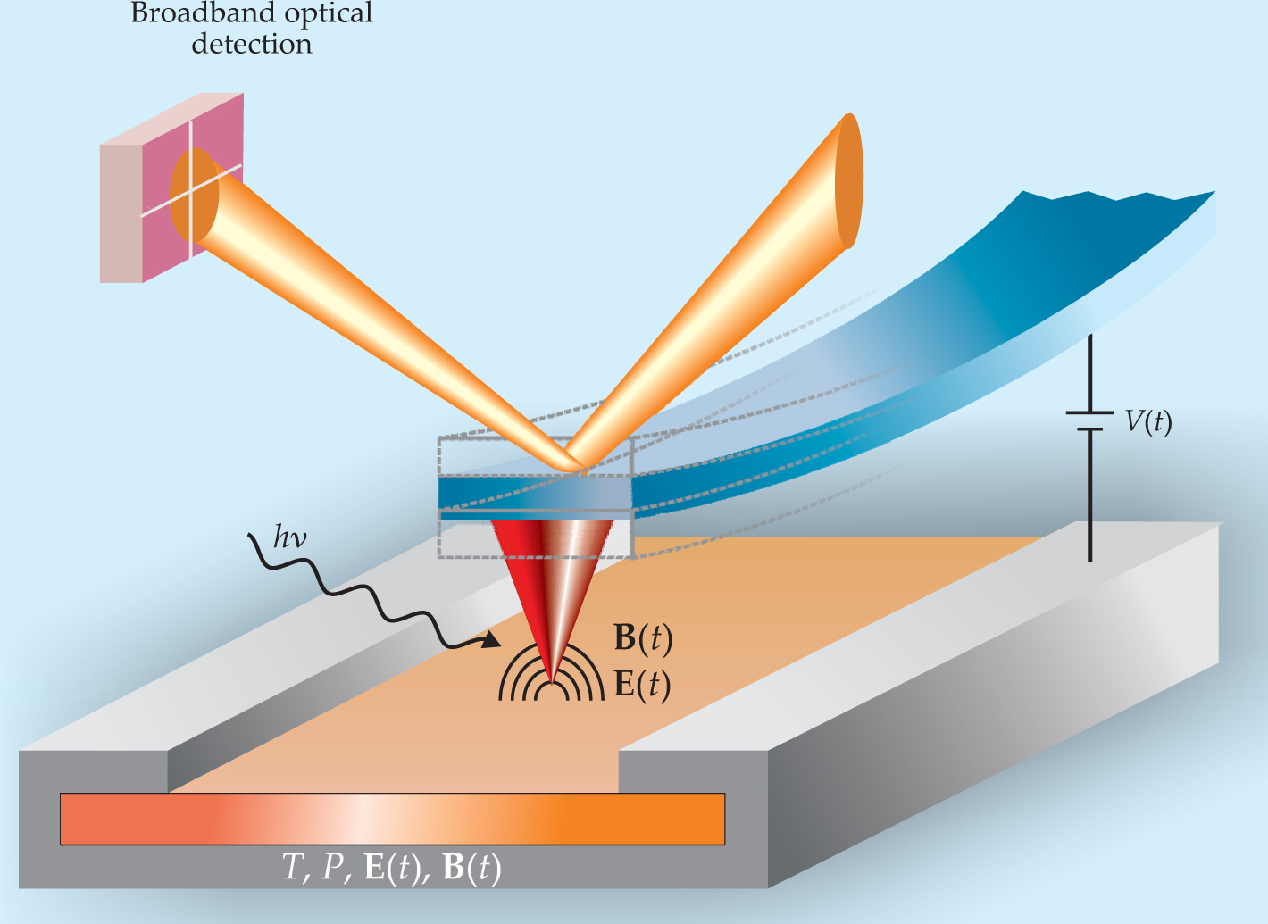
The simple combination of a tip, a surface, and the interaction between them has yielded powerful insights into the spatial distribution of simple material properties, even when the microscope is configured to just map the variations in electromagnetic fields that the tip feels as it scans a surface. But what makes SPM so powerful is the dozens of ways in which the interaction can be tailored—by somehow perturbing the tip or the sample—to investigate additional behaviors of the system. Periodic electrical, magnetic, or mechanical signals can be induced on the tip, for instance, and the frequency dependence or harmonics of the response function can be measured (see figure 1). An alternative to biasing the tip is to apply a lateral field across a surface feature or device component—an approach that facilitates electron-transport measurements.

Figure 1. Interactions between the sharp tip of an atomic force microscope and a sample are rich in information about van der Waals, electrostatic, and magnetic forces. As the tip scans the sample’s surface, the microscope’s electronics monitors the tips vertical and lateral displacement, typically using a laser reflected from the back of a cantilever to a four-quadrant photodetector. The tip may be modulated mechanically (its cantilever driven to vibrate) or electro-magnetically (via an electric field E(t), magnetic field B(t), or photons of energy hv, for instance) to isolate specific material properties. The sample can also be perturbed, possibly at the same time, using pressure P, temperature T, or electromagnetic fields. The photo-detector picks up changes not just in the cantilever’s position but also in its phase and frequency responses, which can be parsed into fundamental and higher-harmonic components. All told, dozens of experimental configurations can be envisioned.
Furthermore, the tip and the sample can be simultaneously excited at multiple frequencies, possibly at the same time. The combinations provide access to a wide range of complex properties, such as piezoelectric coefficients, polarizability, and dopant density. The ability to scan in either contact or noncontact modes further expands the capability.
Surface properties from Coulomb interactions
A charged tip in the presence of a surface with a different electrical potential experiences various forces. Separating the forces by frequency offers a path to directly measure surface potential and the dielectric constant. The tip may be excited with both an oscillating signal V AC at constant frequency ω—much slower than the mechanical resonance—and an adjustable DC signal V DC.
Variations in the cantilever resonance frequency reflect variations in the tip–surface attractive forces ∂F/∂z, where z refers to the tip–surface height. Although the gradient is complex, lock-in amplifiers tuned to the excitation frequency and its harmonics can separate the total force into its constituent parts:
The static term depends on the surface potential and the DC bias on the tip, with V DC – V surf called the contact potential difference. The ω-dependent term vanishes when the CPD does. And the second-harmonic term depends on only the local capacitance C(z) and the magnitude of V AC . Any property inherent in the capacitance can be accessed in that 2ω signal, including intrinsic polarizability and defect energies.
Tip–surface interaction
The tip–surface interaction in the presence of oscillating fields can be quite complex, including as it does chemical-bonding, electrostatic, van der Waals, and magnetic-dipole forces. The
Scanning Kelvin probe microscopy, also known as scanning surface-potential microscopy (SSPM), involves the superposition of both an oscillating bias voltage and a constant one applied to the tip. In the presence of the DC signal, the oscillating bias (at a frequency ω) gives rise to an oscillating mechanical force on the tip in addition to the baseline van der Waals force the tip experiences while vibrating over the surface. As described in the box, the total force gradient on the tip can then be decomposed by lock-in amplifiers into a Coulomb force oscillating at ω and proportional to the tip–sample potential difference, and a capacitive force oscillating at twice that frequency. The surface potential is determined by adjusting the DC tip bias until the frequency shift—and thus the force gradient—that oscillates at ω disappears. Recording the 2ω component of the frequency shift yields a map of surface capacitance.
The approach of manipulating the tip–surface interaction with external fields to isolate particular physical properties is a strategy that can be generalized. In addition to modulations applied to the tip, the sample itself can be perturbed with applied electrical, magnetic, mechanical, or optical fields. Figure 2 illustrates the approach in a comparison between SSPM and scanning impedance microscopy. 2 In SIM, AC and DC voltage biases are applied laterally across the sample, rather than between sample and tip. As the tip responds to local temporal and spatial variations in the electric field above the surface, it creates a map of those responses. The amplitude and phase of the response reflect the local electrical properties of the sample.

Figure 2. Multiple-modulation strategies. (a) Biasing the sample relative to the tip is the foundation for scanning surface-potential microscopy. A feedback loop is used to adjust the DC bias until the amplitude of the force gradient at a frequency ω goes to zero, which gives the local surface potential (see the
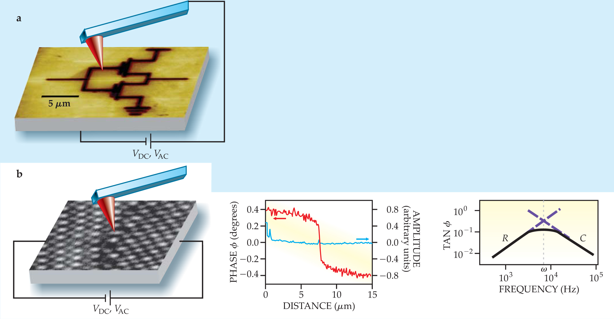
At inhomogeneities such as a diode interface, grain boundary, or atomic defect, the frequency dependence of the sample becomes an experimental tool. In the presence of a lateral AC sample bias, there is no variation in cantilever oscillation amplitude across a grain boundary. However, the phase lag between the current and the excitation voltage is significantly different across the boundary. The phase lag, which at some frequencies is dominated by interface resistance and at others by capacitance, is a consequence of electrons trapped in the interface.
Purely mechanical properties have also been measured with nanometer-scale resolution. In force-modulation AFM, the tip is brought into contact with the sample, which is mechanically oscillated over a range of frequencies. Analyzing the amplitude and phase lag of the cantilever response reveals the stiffness of the tip–surface junction. Researchers have used the method to study the effect of nanostructure geometry on material stiffness for structures as small as 20 nm at a resolution on the order of 10 MPa. 3
Interfacial properties of the tip–surface junction may be similarly probed with contact-mode techniques by adjusting the position of the cantilever to apply compressive or tensile forces to the sample. Reducing the applied load until the tip disengages from the sample yields the system’s interfacial energy, or work of adhesion; the spatial resolution is limited by the contact radius of the junction, typically 1–2 nm. Monitoring the cantilever’s twist as the tip slides across the surface also gives a direct measurement of the friction force and an indirect measurement of the actual contact area. Measurements that plot friction as a function of load thus reveal the shear strength of the interface and other subtleties of the contact mechanics.
Nanometer electronics
Many of the metrology challenges in microelectronics involve understanding how the transport of electrons can vary within device components. Although noncontact AFM offers several advantages, reduced tip wear and an absence of adhesion forces among them, metrologies that involve a current flow require contact between tip and sample. Local conductance, resistance, and capacitance are probed by scanning conductance, spreading resistance, and scanning capacitance microscopies, respectively. In each configuration, a conductive tip scans a voltage-biased surface while the relevant electrical property is recorded.
The spatial resolution is limited both by the physical contact zone and the geometry of electric-field lines. In capacitance measurements, the sharpness of the tip leads to non-trivial fringing fields, an effect that limits resolution to the size of the tip radius. Spreading resistance and conductance microscopies have the opposite problem: When the sample is conductive, current not only flows perpendicularly to the surface but spreads out from the contact zone. Total current thus represents an integration of all paths from the tip to the back plane of the sample. Those considerations led experimentalists to expect that the spatial resolution of capacitance, resistance, and conductance would be limited to roughly 20 nm. It turns out the resolution is much finer than that.
Four years ago Clayton Williams’s group at the University of Utah demonstrated scanning capacitance microscopy (SCM) on voltage-biased transistors and imaged changes in the size and shape of the depletion region in the presence of a local electric field (see figure 3(a)). 4 The smallest features in the device are 20 nm, but SCM has achieved a spatial resolution below 5 nm, approaching the predicted limit of 2 nm for tips with radii of 5–10 nm. 5

Figure 3. Electronic properties of devices. (a) This scanning-capacitance-microscopy image shows the charge-carrier density in an FET. With a bias of +1 V applied by the SCM tip, the source and drain regions (orange) are blocked by a thin layer of material having opposite-polarity carriers (blue). Were the bias voltage changed to −2 V the charge density under the gate would be sufficiently modified to remove the thin junction (also blue) between source and drain and open the channel. (Adapted from ref.
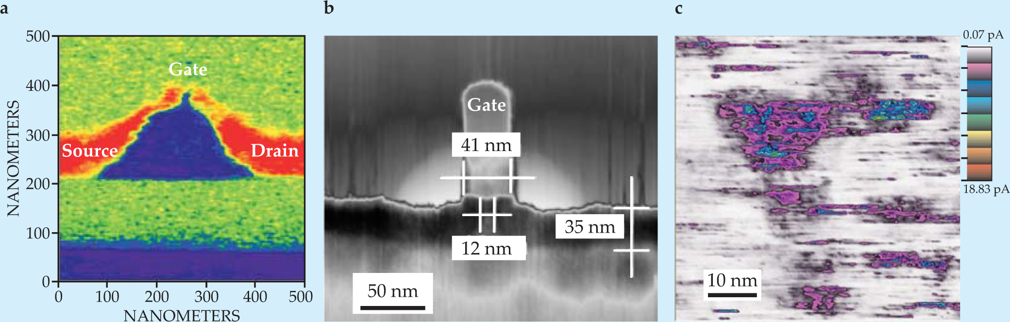
Local resistance has also been mapped in FETs. One strategy to increase device performance is to reduce the size and separation of the transistors. Figure
Some devices are so small that their components can approach atomic dimensions. For example, the insulating film that separates parts of an FET is typically 5 to 8 atomic layers thick. An atomic defect is an appreciable part of that structure and yet can be difficult to detect. Conductive AFM performed on a thin insulating layer above a metallic or semiconductor substrate is similar to STM; the difference is that an insulating layer replaces the air–vacuum gap between tip and surface. Figure
Extracting fundamental properties
The previous examples take the detection of electrical and mechanical properties to unprecedented spatial scales. The measurements can also, at times, access fundamental properties such as polarizability. Recall from the box how capacitance is derived from the second harmonic signal. For a sufficiently simple geometry (a planar surface, for example), measuring capacitance over a large frequency range directly yields the dielectric function and atomic polarizability. In nanostructures such as quantum wires, tubes, and dots, low dimensionality gives rise to quantum behavior. The measured capacitance could include contributions from quantum capacitance, Coulomb blockades, and abrupt variations and singularities in densities of states.
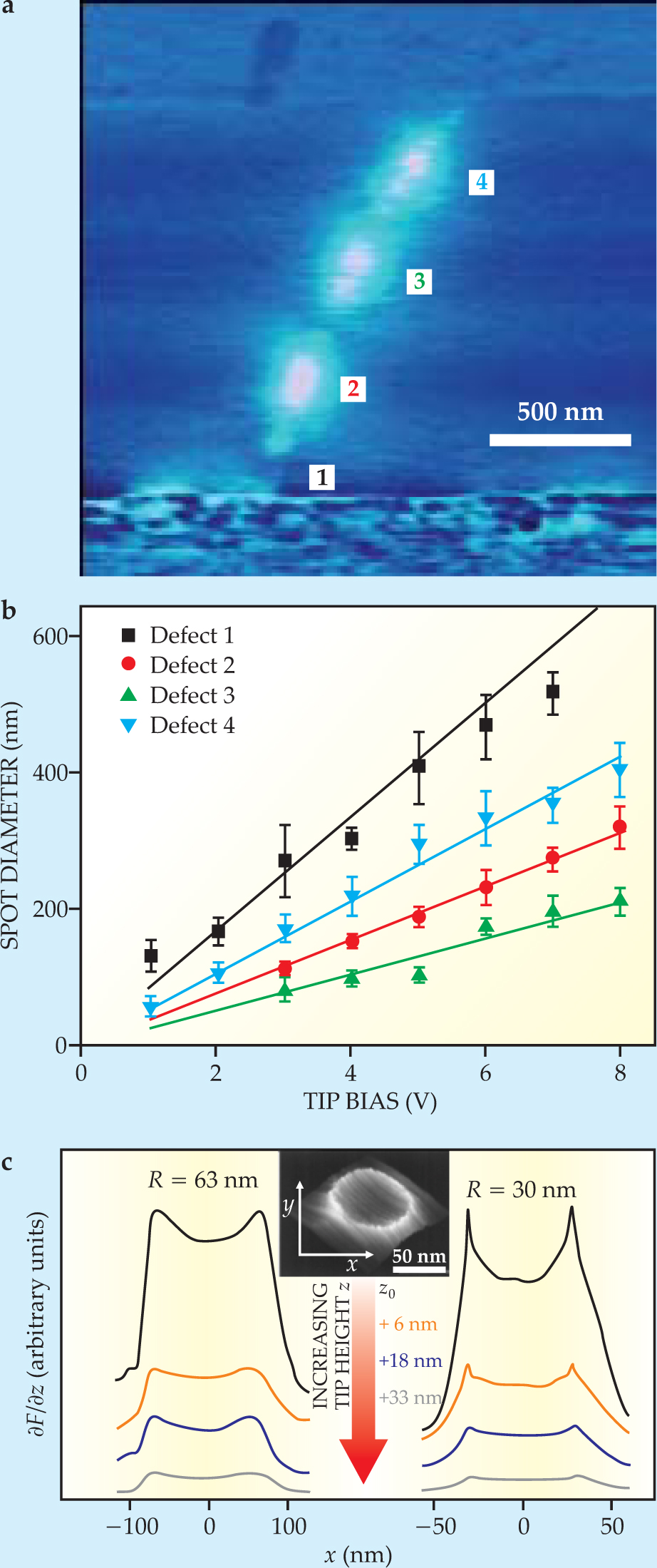
The last of those contributions is illustrated in figures 4(a) and

Figure 4. Properties of nanotubes and nanowires. (a) This scanning impedance micrograph reveals current flowing though a carbon nanotube containing four defects. The tip is held at 4 V. (b) The apparent size of each defect increases linearly with the bias voltage applied to the tip. The slope of each line determines the local valence-band energy due to the corresponding defect. (Adapted from ref.
(Adapted from ref. 9.)
Nearly a decade ago the MIT group led by Mildred Dresselhaus and Gene Dresselhaus probed quasi-one-dimensional confined states in bismuth quantum wires. By standing Bi nanowires on end, they effectively reproduced the particle-in-a-box problem and used a DC-biased tip in noncontact AFM to map charge density across the flat end of the nanowire.
9
Confined electrons on the surface interact with the tip to enhance the local force gradient and are consequently detectable. The team examined the competition between electrostatics and the quantum mechanical particle-in-a-box solution, with electrons predicted to reside near the center of the potential well. Figure
Complexity and anisotropy
Most properties of solids are not scalar but rather tensor quantities. They vary with direction and in some cases are interdependent with other properties. Piezoelectricity, as noted earlier, involves a connection between mechanical strain and electric field in a material. Piezoresponse force microscopy (PFM) combines contact-mode scanning with AC-voltage biasing of the tip to characterize the electromechanical properties of materials that expand and contract in response to an external field. In ferroelectric materials the inherent electrical dipoles are coupled and form domains. Because ferroelectric domains exhibit piezoelectric responses, PFM can characterize the domains locally.
Until recently, it was only possible to determine the properties of individual domains in two dimensions at once: normal to the surface and laterally, relative to the cantilever’s axis. Sergei Kalinin’s group at Oak Ridge National Laboratory has recently developed a technique to decouple three simultaneous modes of AFM cantilever deflection: out-of-plane bending, lateral torsion, and longitudinal buckling. 10 The three modes roughly correspond to material displacements along three axes.
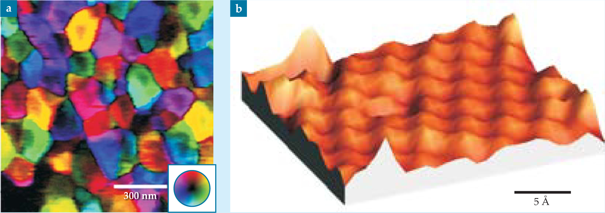
Isolating the mechanical responses to electrical-field variation explicitly probes the direction dependence of the piezoelectric coupling between strain and electric field. A map in the form of a color wheel can indicate direction and intensity of the polarization vector in two or three dimensions and provide a richly detailed graphical representation of the local properties (see figure 5). That contact-mode method routinely exhibits 30-nm resolution, but Kalinin’s team reached a resolution better than 5 nm by imaging a protein in water to screen spurious electrostatic effects. Although that achievement was not intuitive, researchers using STM and AFM can obtain nearly atomically resolved images of functional materials such as barium titanate.

Figure 5. This piezoresponse force microscopy image (a) reveals barium titanate’s response to an applied electric field. The colors represent the magnitude and direction of surface displacement in two dimensions for individual domains. Black represents zero response and colors indicate lateral and vertical displacement according to the wheel in the lower right-hand corner. (Adapted from ref.
(Adapted from D. A. Bonnell, J. Garra,
Toward the ultimate limit
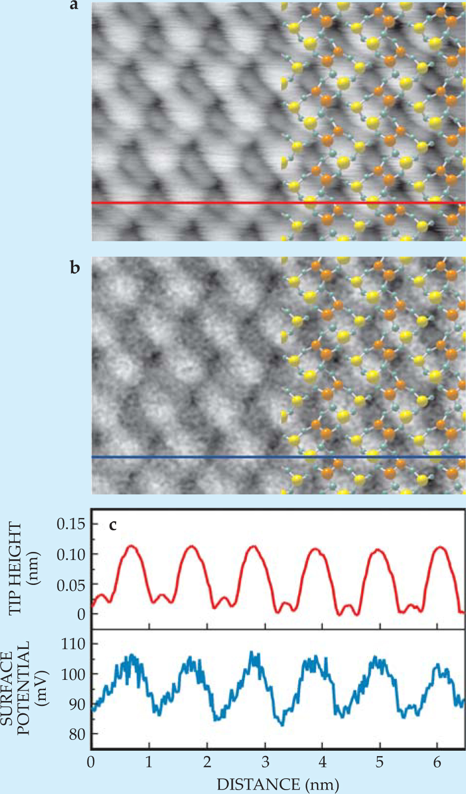
What properties might be measurable with single-atom resolution? One could take a reductionist view and consider electronic structure, which STM routinely images, as a property itself. Examples include Donald Eigler’s iconic quantum corrals, Séamus Davis’s superconducting bandgap maps, and the imaging of charge density waves. But what determines the limits for continuum material properties? Only recently have single charges and single electron spins been detected with scanning probe methods (see Physics Today, September 2004, page 21 ). And groups led by the University of Tokyo’s Yukio Hasegawa and Tohoku University’s Yasuo Cho have demonstrated atomic-resolution mapping of surface potential on germanium 11 and silicon, 12 respectively. Figure 6 demonstrates high-resolution noncontact-AFM imaging of a reconstructed Ge surface. Atoms with different numbers of dangling bonds occupy different sites on the surface, and the differences are obvious in STM and NC-AFM images. Simultaneously acquired surface-potential maps, with an energy resolution of about 3 meV, correlate high surface potential with rebonded atoms that have a lower number of dangling bonds.

Figure 6. Noncontact atomic force microscopy resolves the (1 × 2) atomic reconstruction (a) of a germanium surface. Simultaneously, the microscope’s tip measures variations in the surface potential (b) during the scan. Yellow atoms are ones that rebonded during the reconstruction; orange atoms have dangling bonds and consequently a lower work function. (c) The topography (red) and potential (blue) along the same section of the surface.
(Adapted from ref. 11.)
Cases in which surface properties can be imaged at atomic resolution are sure to challenge our understanding of materials and raise intriguing questions. What complicates image interpretation is that interactions at the tip–surface junction are a superposition of atomic bonding and local properties of the material itself. Untangling those properties from the tip’s contribution may be difficult. In any case, new definitions of what the term “property” really means may be necessary as researchers explore the transition between continuum and atomic realms. In some instances the transition seems obvious: from dielectric constant to atomic polarizability or from work function to ionization potential. But the practical realization, no doubt, will be complex.
References
1. D. D. Bonnell, ed., Scanning Probe Microscopy and Spectroscopy: Theory, Techniques, and Applications, 2nd ed., Wiley-VCH, New York (2001).
2. R. Shao, S. S. Kalinin, D. D. Bonnell, Appl. Phys. Lett. 82, 1869 (2003).https://doi.org/APPLAB
10.1063/1.1561168 3. W. W. Price et al., J. Phys. Chem. A 110, 1382 (2006).https://doi.org/JPCAFH
10.1021/jp0544540 4. E. Bussmann, C. C. Williams, Rev. Sci. Instrum. 75, 422 (2004).https://doi.org/RSINAK
10.1063/1.1641161 5. S. Lanyi, M. Hruskovic, J. Phys. D: Appl. Phys. 36, 598 (2003).https://doi.org/JPAPBE
10.1088/0022-3727/36/5/326 6. P. Eyben, T. Janssens, W. Vandervorst, Mater. Sci. Eng. B 124, 45 (2005).https://doi.org/MSBTEK
10.1016/j.mseb.2005.08.049 7. M. Freitag et al., Phys. Rev. Lett. 89, 216801 (2002).https://doi.org/PRLTAO
10.1103/PhysRevLett.89.216801 8. M. M. Woodside, P. P. McEuen, Science 296, 1098 (2002).https://doi.org/SCIEAS
10.1126/science.1069923 9. D. Gekhtman et al., Phys. Rev. Lett. 82, 3887 (1999).https://doi.org/PRLTAO
10.1103/PhysRevLett.82.3887 10. S. S. Kalinin et al., Microsc. Microanal. 12, 206 (2006).https://doi.org/MIMIF7
10.1017/S1431927606060156 11. T. Eguchi et al., Phys. Rev. Lett. 93, 266102 (2004).https://doi.org/PRLTAO
10.1103/PhysRevLett.93.266102 12. Y. Cho, R. Hirose, Phys. Rev. Lett. 99, 186101 (2007).https://doi.org/PRLTAO
10.1103/PhysRevLett.99.186101
More about the authors
Matt Brukman is a postdoctoral fellow and Dawn Bonnell a Trustee Professor in the department of materials science and engineering at the University of Pennsylvania in Philadelphia.
Matthew J. Brukman, University of Pennsylvania in Philadelphia, US .
Dawn A. Bonnell, University of Pennsylvania in Philadelphia, US .


